128 KByte Flash Module (S12FTMRC128K1V1)
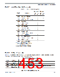
Table 13-29. D-Flash Commands
FCMD
Command
Function on D-Flash Memory
Erase Verify D-
Flash Section
Verify that a given number of words starting at the address provided are erased.
0x10
0x11
0x12
Program D-Flash
Program up to four words in the D-Flash block.
Erase all bytes in a sector of the D-Flash block.
Erase D-Flash
Sector
13.4.4 Allowed Simultaneous P-Flash and D-Flash Operations
Only the operations marked ‘OK’ in Table 13-30 are permitted to be run simultaneously on the Program
Flash and Data Flash blocks. Some operations cannot be executed simultaneously because certain
hardware resources are shared by the two memories. The priority has been placed on permitting Program
Flash reads while program and erase operations execute on the Data Flash, providing read (P-Flash) while
write (D-Flash) functionality.
Table 13-30. Allowed P-Flash and D-Flash Simultaneous Operations
Data Flash
Margin
Read1
Sector
Erase
Mass
Program Flash
Read
Read
Program
Erase3
OK
OK
OK
Margin Read(1)
Program
OK(2)
Sector Erase
OK
Mass Erase(3)
OK
1. A ‘Margin Read’ is any read after executing the margin setting commands ‘Set
User Margin Level’ or ‘Set Field Margin Level’ with anything but the ‘normal’
level specified.
2. See the Note on margin settings in Section 13.4.5.12 and Section 13.4.5.13.
3. The ‘Mass Erase’ operations are commands ‘Erase All Blocks’ and ‘Erase
Flash Block’
13.4.5 Flash Command Description
This section provides details of all available Flash commands launched by a command write sequence. The
ACCERR bit in the FSTAT register will be set during the command write sequence if any of the following
illegal steps are performed, causing the command not to be processed by the Memory Controller:
•
Starting any command write sequence that programs or erases Flash memory before initializing the
FCLKDIV register
•
•
Writing an invalid command as part of the command write sequence
For additional possible errors, refer to the error handling table provided for each command
S12P-Family Reference Manual, Rev. 1.13
Freescale Semiconductor
455

 FREESCALE [ Freescale ]