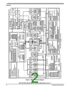
Features
— Retires as many as three instructions per clock cycle
Separate on-chip L1 instruction and data caches (Harvard architecture)
— 32-Kbyte, eight-way set-associative instruction and data caches
— Pseudo least-recently-used (PLRU) replacement algorithm
— 32-byte (eight-word) L1 cache block
•
— Physically indexed/physical tags
— Cache write-back or write-through operation programmable on a per-page or per-block basis
— Instruction cache can provide four instructions per clock cycle; data cache can provide four words per
clock cycle
— Caches can be disabled in software
— Caches can be locked in software
— MESI data cache coherency maintained in hardware
— Separate copy of data cache tags for efficient snooping
— Parity support on cache and tags
— No snooping of instruction cache except for icbi instruction
— Data cache supports AltiVec LRU and transient instructions
— Critical double- and/or quad-word forwarding is performed as needed. Critical quad-word forwarding
is used for AltiVec loads and instruction fetches. Other accesses use critical double-word forwarding.
•
Level 2 (L2) cache interface
— On-chip, 256-Kbyte, eight-way set-associative unified instruction and data cache
— Fully pipelined to provide 32 bytes per clock cycle to the L1 caches
— A total nine-cycle load latency for an L1 data cache miss that hits in L2
— PLRU replacement algorithm
— Cache write-back or write-through operation programmable on a per-page or per-block basis
— 64-byte, two-sectored line size
— Parity support on cache
•
Level 3 (L3) cache interface (not implemented on MPC7445)
— Provides critical double-word forwarding to the requesting unit
— Internal L3 cache controller and tags
— External data SRAMs
— Support for 1- and 2-Mbyte L3 caches
— Cache write-back or write-through operation programmable on a per-page or per-block basis
— 64-byte (1M) or 128-byte (2M) sectored line size
— Private memory capability for half (1-Mbyte minimum) or all of the L3 SRAM space
— Supports MSUG2 dual data rate (DDR) synchronous Burst SRAMs, PB2 pipelined synchronous Burst
SRAMs, and pipelined (register-register) late write synchronous Burst SRAMs
— Supports parity on cache and tags
— Configurable core-to-L3 frequency divisors
— 64-bit external L3 data bus sustains 64 bits per L3 clock cycle
MPC7455 RISC Microprocessor Hardware Specifications, Rev. 4.1
Freescale Semiconductor
5

 FREESCALE [ Freescale ]