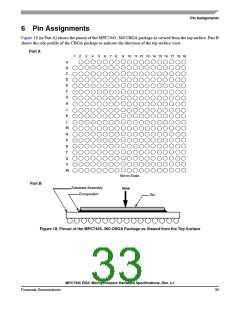
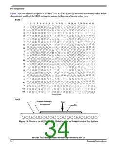
Pinout Listings
7 Pinout Listings
Table 15 provides the pinout listing for the MPC7445, 360 CBGA package. Table 16 provides the pinout listing for
the MPC7455, 483 CBGA package.
NOTE
This pinout is not compatible with the MPC750, MPC7400, or MPC7410, 360
BGA package.
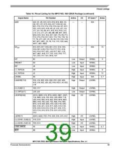
Table 15. Pinout Listing for the MPC7445, 360 CBGA Package
1
Signal Name
A[0:35]
Pin Number
Active
I/O
I/F Select
Notes
E11, H1, C11, G3, F10, L2, D11, D1, C10,
G2, D12, L3, G4, T2, F4, V1, J4, R2, K5,
W2, J2, K4, N4, J3, M5, P5, N3, T1, V2,
U1, N5, W1, B12, C4, G10, B11
High
I/O
BVSEL
11
AACK
R1
Low
High
Low
—
Input
I/O
BVSEL
BVSEL
BVSEL
N/A
AP[0:4]
ARTRY
C1, E3, H6, F5, G7
N2
A8
M1
G9
F8
D2
B7
J1
I/O
8
AV
Input
Input
Input
Input
Output
Input
Output
Input
Output
Output
I/O
DD
BG
Low
Low
Low
Low
High
Low
Low
Low
High
High
BVSEL
BVSEL
BVSEL
BVSEL
BVSEL
BVSEL
BVSEL
BVSEL
BVSEL
BVSEL
BMODE0
BMODE1
BR
5
6
BVSEL
CI
1, 7
8
CKSTP_IN
CKSTP_OUT
CLK_OUT
D[0:63]
A3
B1
H2
R15, W15, T14, V16, W16, T15, U15,
P14, V13, W13, T13, P13, U14, W14,
R12, T12, W12, V12, N11, N10, R11, U11,
W11, T11, R10, N9, P10, U10, R9, W10,
U9, V9, W5, U6, T5, U5, W7, R6, P7, V6,
P17, R19, V18, R18, V19, T19, U19, W19,
U18, W17, W18, T16, T18, T17, W3, V17,
U4, U8, U7, R7, P6, R8, W8, T8
DBG
M2
Low
High
Low
High
High
Input
I/O
BVSEL
BVSEL
BVSEL
BVSEL
BVSEL
DP[0:7]
DRDY
T3, W4, T4, W9, M6, V3, N8, W6
R3
Output
Input
Input
4
13
9
DTI[0:3]
EXT_QUAL
G1, K1, P1, N1
A11
MPC7455 RISC Microprocessor Hardware Specifications, Rev. 4.1
Freescale Semiconductor
35

 FREESCALE [ Freescale ]