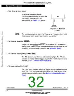
Freescale Semiconductor, Inc.
Memory
subroutine call to save the CPU state. The stack pointer decrements
during pushes and increments during pulls.
Figure 2-1 is a memory map of the MCU. Addresses $0000–$001F,
shown in Figure 2-2, contain most of the control, status, and data
registers. Additional I/O registers have these addresses:
• $1FDF, option register
• $1FF0, mask option register 1 (MOR1)
• $1FF1, mask option register 2 (MOR2)
2.4 Input/Output (I/O)
The first 32 addresses of memory space, from $0000 to $001F, are the
I/O section. These are the addresses of the I/O control registers, status
registers, and data registers. See Figure 2-2 for more information.
2.5 RAM
One of four selectable memory configurations is selected by the state of
the RAM1 and RAM0 bits in the option register located at $1FDF. Reset
or power-on reset (POR) clears these bits, automatically selecting the
first memory configuration as shown in Table 2-1. See 9.5.1 Option
Register.
Table 2-1. Memory Configurations
RAM0
RAM1
RAM Bytes
176
PROM Bytes
7744
0
1
0
1
0
0
1
1
208
7696
272
7648
304
7600
NOTE: Be careful when using nested subroutines or multiple interrupt levels.
The CPU can overwrite data in the stack RAM during a subroutine or
during the interrupt stacking operation.
Technical Data
36
MC68HC705C8A — Rev. 3
Memory
For More Information On This Product,
Go to: www.freescale.com

 FREESCALE [ Freescale ]