Freescale Semiconductor, Inc.
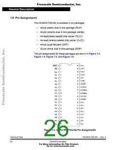
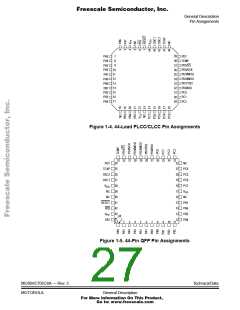
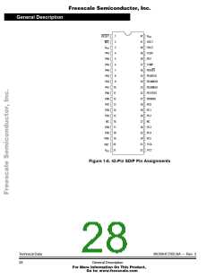
General Description
RAM0 — Random-Access Memory Control Bit 0
1 = Maps 32 bytes of RAM into page zero starting at address
$0030. Addresses from $0020 to $002F are reserved. This bit
can be read or written at any time, allowing memory
configuration to be changed during program execution.
0 = Provides 48 bytes of PROM at location $0020–$005F.
RAM1 — Random-Access Memory Control Bit 1
1 = Maps 96 bytes of RAM into page one starting at address $0100.
This bit can be read or written at any time, allowing memory
configuration to be changed during program execution.
0 = Provides 96 bytes of PROM at location $0100.
SEC — Security Bit
This bit is implemented as an erasable, programmable read-only
memory (EPROM) cell and is not affected by reset.
1 = Bootloader disabled; MCU operates only in single-chip mode
0 = Security off; bootloader can be enabled
IRQ — Interrupt Request Pin Sensitivity Bit
IRQ is set only by reset, but can be cleared by software. This bit can
be written only once.
1 = IRQ pin is both negative edge- and level-sensitive.
0 = IRQ pin is negative edge-sensitive only.
Bits 5, 4, and 0 — Not used; always read 0
Bit 2 — Unaffected by reset; reads either 1 or 0
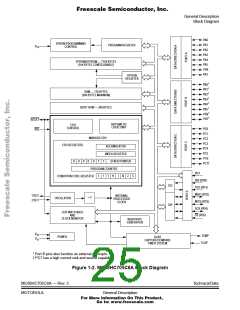
1.5 Block Diagram
Figure 1-2 shows the structure of the MC68HC705C8A.
Technical Data
24
MC68HC705C8A — Rev. 3
General Description
For More Information On This Product,
Go to: www.freescale.com

 FREESCALE [ Freescale ]