Freescale Semiconductor, Inc.
Instruction Set
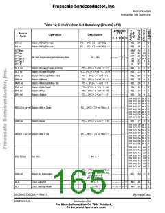
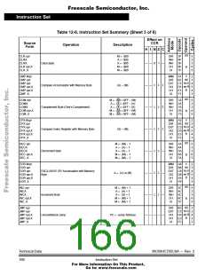
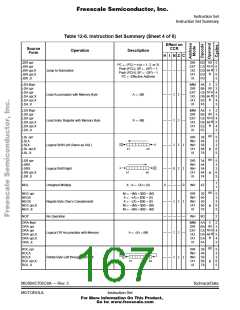
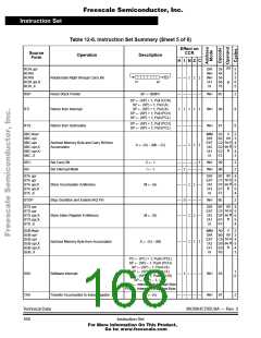
Opcode Map
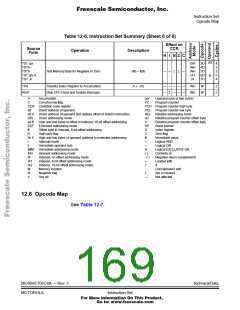
Table 12-6. Instruction Set Summary (Sheet 6 of 6)
e
Effect on
s
e
Source
Form
CCR
r
Operation
Description
d
cod
d
M
H I N Z C
C
p
d
Ope
dd
ff
TST opr
TSTA
TSTX
TST opr,X
TST ,X
DIR
INH
INH
IX1
IX
3D
4D
5D
6D
7D
4
3
3
5
4
Test Memory Byte for Negative or Zero
(M) – $00
— —
—
TXA
Transfer Index Register to Accumulator
Stop CPU Clock and Enable Interrupts
A ← (X)
— — — — —
— — — —
INH
INH
9F
8F
2
2
WAIT
A
C
Accumulator
Carry/borrow flag
opr
PC
Operand (one or two bytes)
Program counter
CCR Condition code register
PCH Program counter high byte
PCL Program counter low byte
REL Relative addressing mode
dd
Direct address of operand
dd rr
DIR
ee ff
EXT
ff
Direct address of operand and relative offset of branch instruction
Direct addressing mode
High and low bytes of offset in indexed, 16-bit offset addressing
Extended addressing mode
Offset byte in indexed, 8-bit offset addressing
Half-carry flag
rel
rr
SP
X
Relative program counter offset byte
Relative program counter offset byte
Stack pointer
Index register
H
Z
Zero flag
hh ll
I
High and low bytes of operand address in extended addressing
Interrupt mask
#
Immediate value
Logical AND
ii
Immediate operand byte
Logical OR
IMM
INH
IX
IX1
IX2
M
Immediate addressing mode
Inherent addressing mode
Indexed, no offset addressing mode
Indexed, 8-bit offset addressing mode
Indexed, 16-bit offset addressing mode
Memory location
Logical EXCLUSIVE OR
Contents of
Negation (two’s complement)
Loaded with
( )
–( )
←
?
If
:
Concatenated with
Set or cleared
N
Negative flag
n
Any bit
—
Not affected
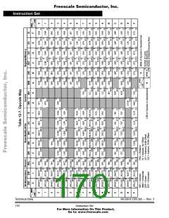
12.6 Opcode Map
See Table 12-7.
MC68HC705C8A — Rev. 3
MOTOROLA
Technical Data
Instruction Set
For More Information On This Product,
Go to: www.freescale.com

 FREESCALE [ Freescale ]