Freescale Semiconductor, Inc.
Instruction Set
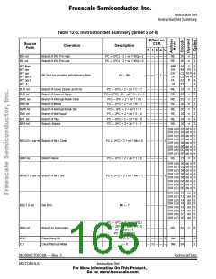
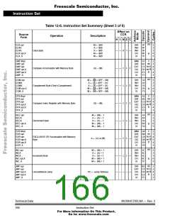
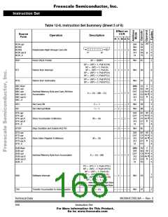
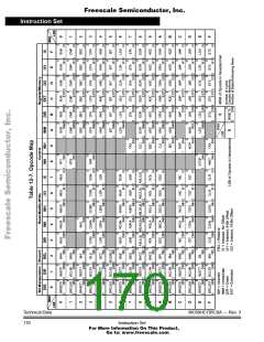
Instruction Set Summary
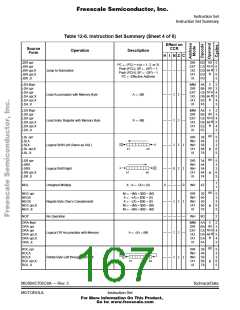
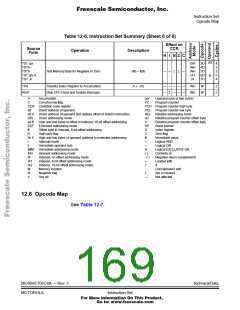
Table 12-6. Instruction Set Summary (Sheet 4 of 6)
e
Effect on
s
e
Source
Form
CCR
r
Operation
Description
d
cod
d
M
H I N Z C
C
p
d
Ope
dd
hh ll
ee ff
ff
JSR opr
DIR
BD
CD
DD
ED
FD
5
6
7
6
5
PC ← (PC) + n (n = 1, 2, or 3)
Push (PCL); SP ← (SP) – 1
Push (PCH); SP ← (SP) – 1
PC ← Effective Address
JSR opr
JSR opr,X
JSR opr,X
JSR ,X
EXT
IX2
IX1
IX
Jump to Subroutine
— — — — —
ii
dd
hh ll
ee ff
ff
LDA #opr
LDA opr
LDA opr
LDA opr,X
LDA opr,X
LDA ,X
IMM
DIR
EXT
IX2
IX1
IX
A6
B6
C6
D6
E6
F6
2
3
4
5
4
3
Load Accumulator with Memory Byte
A ← (M)
X ← (M)
— —
—
—
ii
dd
hh ll
ee ff
ff
LDX #opr
LDX opr
LDX opr
LDX opr,X
LDX opr,X
LDX ,X
IMM
DIR
EXT
IX2
IX1
IX
AE
BE
CE
DE
EE
FE
2
3
4
5
4
3
Load Index Register with Memory Byte
Logical Shift Left (Same as ASL)
— —
dd
LSL opr
LSLA
LSLX
LSL opr,X
LSL ,X
DIR
INH
INH
IX1
IX
38
48
58
68
78
5
3
3
6
5
C
0
— —
b7
b0
ff
dd
LSR opr
LSRA
LSRX
LSR opr,X
LSR ,X
DIR
INH
INH
IX1
IX
34
44
54
64
74
5
3
3
6
5
0
C
Logical Shift Right
Unsigned Multiply
— — 0
b7
b0
ff
1
1
MUL
X : A ← (X) × (A)
0 — — — 0
INH
42
dd
ff
NEG opr
NEGA
NEGX
NEG opr,X
NEG ,X
M ← –(M) = $00 – (M)
A ← –(A) = $00 – (A)
X ← –(X) = $00 – (X)
M ← –(M) = $00 – (M)
M ← –(M) = $00 – (M)
DIR
INH
INH
IX1
IX
30
40
50
60
70
5
3
3
6
5
Negate Byte (Two’s Complement)
No Operation
— —
NOP
— — — — —
INH
9D
2
ii
dd
hh ll
ee ff
ff
ORA #opr
ORA opr
ORA opr
ORA opr,X
ORA opr,X
ORA ,X
IMM
DIR
EXT
IX2
IX1
IX
AA
BA
CA
DA
EA
FA
2
3
4
5
4
3
Logical OR Accumulator with Memory
Rotate Byte Left through Carry Bit
A ← (A) (M)
— —
—
dd
ff
ROL opr
ROLA
ROLX
ROL opr,X
ROL ,X
DIR
INH
INH
IX1
IX
39
49
59
69
79
5
3
3
6
5
C
— —
b7
b0
MC68HC705C8A — Rev. 3
MOTOROLA
Technical Data
Instruction Set
For More Information On This Product,
Go to: www.freescale.com

 FREESCALE [ Freescale ]