Freescale Semiconductor, Inc.
EPROM/OTPROM (PROM)
9.5 Control Registers
This subsection describes the three registers that control memory
configuration, PROM security, and IRQ edge or level sensitivity; port B
pullups; and non-programmable COP enable/disable.
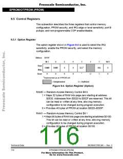
9.5.1 Option Register
The option register shown in Figure 9-4 is used to select the IRQ
sensitivity, enable the PROM security, and select the memory
configuration.
Address: $1FDF
Bit 7
RAM0
0
6
RAM1
0
5
0
0
4
0
0
3
SEC*
*
2
1
IRQ
1
Bit 0
0
Read:
Write:
Reset:
U
0
*Implemented as an EPROM cell
= Unimplemented
U = Unaffected
Figure 9-4. Option Register (Option)
RAM0 — Random-Access Memory Control Bit 0
1 = Maps 32 bytes of RAM into page zero starting at address
$0030. Addresses from $0020 to $002F are reserved. This bit
can be read or written at any time, allowing memory
configuration to be changed during program execution.
0 = Provides 48 bytes of PROM at location $0020–$005F.
RAM1 — Random-Access Memory Control Bit 1
1 = Maps 96 bytes of RAM into page one starting at address $0100.
This bit can be read or written at any time, allowing memory
configuration to be changed during program execution.
0 = Provides 96 bytes of PROM at location $0100.
Technical Data
116
MC68HC705C8A — Rev. 3
EPROM/OTPROM (PROM)
For More Information On This Product,
Go to: www.freescale.com

 FREESCALE [ Freescale ]