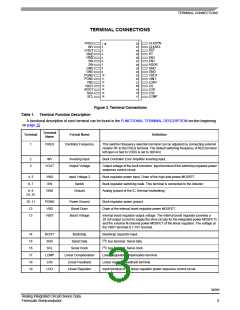
TERMINAL CONNECTIONS
TERMINAL CONNECTIONS
FREQ
CLKSYN
CLKSEL
RST
RT
EN2
1
32
31
30
29
28
27
26
25
24
23
22
21
20
19
18
17
INV
VOUT
VIN2
VIN2
SW
2
3
4
5
6
EN1
7
SW
ADDR
GND
GND
VDD1
VIN1
LDRV
CS
LDO
LFB
LCMP
8
GND
GND
PGND
PGND
VBD
VBST
BOOT
SDA
9
10
11
12
13
14
15
16
SCL
Figure 3. Terminal Connections
Table 1. Terminal Function Description
A functional description of each terminal can be found in the FUNCTIONAL TERMINAL DESCRIPTION section beginning
on page 15.
Terminal
Name
Terminal
Formal Name
Definition
1
FREQ
Oscillator Frequency
This switcher frequency selection terminal can be adjusted by connecting external
resistor RF to the FREQ terminal. The default switching frequency (FREQ terminal
left open or tied to VDDI) is set to 300 kHz.
2
3
INV
Inverting Input
Output Voltage
Buck Controller Error Amplifier inverting input.
VOUT
Output voltage of the buck converter. Input terminal of the switching regulator power
sequence control circuit.
4, 5
6, 7
VIN2
SW
Input Voltage 2
Switch
Buck regulator power input. Drain of the high-side power MOSFET.
Buck regulator switching node. This terminal is connected to the inductor.
Analog ground of the IC, thermal heatsinking.
8, 9
GND
Ground
24, 25
10, 11
12
PGND
VBD
Power Ground
Boost Drain
Buck regulator power ground.
Drain of the internal boost regulator power MOSFET.
13
VBST
Boost Voltage
Internal boost regulator output voltage. The internal boost regulator provides a
20 mA output current to supply the drive circuits for the integrated power MOSFETs
and the external N-channel power MOSFET of the linear regulator. The voltage at
the VBST terminal is 7.75V nominal.
14
15
16
17
18
19
BOOT
SDA
SCL
Bootstrap
Serial Data
Bootstrap capacitor input.
I2C bus terminal. Serial data.
Serial Clock
I2C bus terminal. Serial clock.
LCMP
LFB
Linear Compensation
Linear Feedback
Linear Regulator
Linear regulator compensation terminal.
Linear regulator feedback terminal.
Input terminal of the linear regulator power sequence control circuit.
LDO
34701
Analog Integrated Circuit Device Data
Freescale Semiconductor
3

 FREESCALE [ Freescale ]