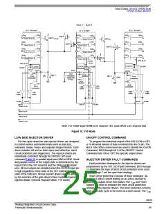
FUNCTIONAL DEVICE OPERATION
OPERATIONAL MODES
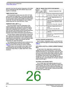
faults. Timing between two write words must be greater than
the fault timer to allow adequate time to sense and report the
proper fault status.
SPI RESPONSE REGISTERS
Fault reporting is accomplished through the SPI interface.
All logic [1]s received by the MCU via the SO pin indicate
faults. All logic [0]s received by the MCU via Pin indicate no
.
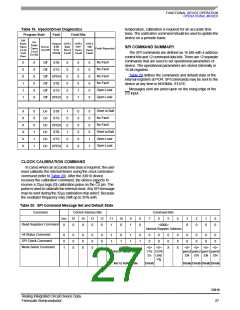
Table 21. SPI Response Messages
15
0
14
0
13
0
12
0
11
1
10
1
9
0
8
1
7
0
6
0
5
0
4
0
3
1
2
0
1
1
0
0
Next SO Response to:
SPI Check Command
Next SO Response to
HEX1 to HEX A
Reset COR SOR
NMF IGN3 IGN2 IGN1 IGN0 GP3 GP2 GP1 GP0 OUT3 OUT2 OUT1 OUT0
Fault Fault Fault Fault Fault Fault Fault Fault Fault Fault Fault Fault
Commands and Read All
Status Command
ALL STATUS
RESPONSE
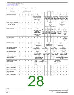
Next SO Response to
READ REGISTER
COMMAND
15
14
13
12
11
10
9
8
7
6
5
4
3
2
1
0
Address <0000>
All Status Register
0 = No Fault, 1 = Fault
Reset COR SOR
NMF IGN3 IGN2 IGN1 IGN0 GP3 GP2 GP1 GP0 OUT3 OUT2 OUT1 OUT0
Fault Fault Fault Fault Fault Fault Fault Fault Fault Fault Fault Fault
Address <0001>
OUT1, OUT0 Fault
Register
Reset COR OVER LOW
Voltage Voltage
0
0
0
0
0
0
0
0
0
0
0
0
OUT1 OUT1 OUT1 OUT1 OUT0 OUT0 OUT0 OUT0
TLIM Batter OFF ON TLIM Batter OFF ON
Fault
y
Open Open Fault
y
Open Open
0 = No Fault, 1 = Fault
Short Fault Fault
Fault
Short Fault Fault
Fault
Address <0010>
OUT3, OUT2 Fault
Register
Reset COR OVER LOW
Voltage Voltage
OUT3 OUT3 OUT3 OUT3 OUT2 OUT2 OUT2 OUT2
TLIM Batter OFF ON TLIM Batter OFF ON
Fault
y
Open Open Fault
y
Open Open
0 = No Fault, 1 = Fault
Short Fault Fault
Fault
Short Fault Fault
Fault
Address <0011>
GPGD Mode Fault
Register
Reset COR OVER LOW
Voltage Voltage
GP3 GP3 GP2 GP2 GP1 GP1 GP0 GP0
Short Open Short Open Short Open Short Open
Circuit Load Circuit Load Circuit Load Circuit Load
Fault Fault Fault Fault Fault Fault Fault Fault
0 = No Fault, 1 = Fault
Address <0100>
IGN Mode Fault Register
0 = No Fault, 1 = Fault
Reset COR OVER LOW IGN3 IGN3 IGN3 IGN2 IGN2 IGN2 IGN1 IGN1 IGN1 IGN0 IGN0 IGN0
Voltage Voltage MAXI Max Open MAXI Max Open MAXI Max Open MAXI Max Open
Fault Dwell Secon Fault Dwell Secon Fault Dwell Secon Fault Dwell Secon
Fault
d
Fault
d
Fault
d
Fault
d
Fault
Fault
Fault
Fault
Address <0101>
Mode Command Register
Reset COR OVER LOW
Voltage Voltage
IGN/GP Mode Select
V10 OVR
En Vtg
X
X
PWM PWM PWM PWM
3
2
1
0
EN
EN
EN
EN
Address <0110>
LSD Fault Command
Register
Reset COR OVER LOW LSD Flt Operation
Voltage Voltage shutdn,Tlim,Timer
X
X
OUT3 OUT2 OUT1 OUT0 OUT3 OUT2 OUT1 OUT0
ON ON ON ON OFF OFF OFF OFF
Open Open Open Open Open Open Open Open
Load Load Load Load Load Load Load Load
Reset COR OVER LOW
Voltage Voltage
X
X
X
GPGD(19)
OUTx Driver(19)
Address <0111>
Drvr ON/OFF Command
Reg
Address <1000>
Spark Command Register
Reset COR OVER LOW
Voltage Voltage
Max Dwell Timer
MaxDwell
Max Over Gain Soft Open
Dwell lap
En Dwell
Open
Secondary
End Spark
Threshold
Sel Shut 2ed
Dn En Clmp
Notes
19. These bits refer to command On or Off state in the command registers, not the state of the respective output lines. These bits are not to be
confused with the ignition mode state which is controlled only by the parallel inputs and their state is not reflected in these bits.
33810
Analog Integrated Circuit Device Data
Freescale Semiconductor
29

 FREESCALE [ Freescale ]