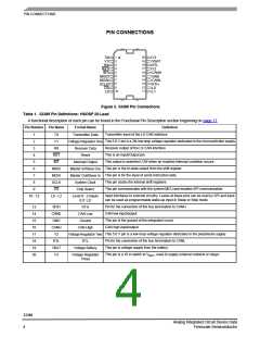
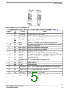
PIN CONNECTIONS
PIN CONNECTIONS
1
20
19
18
17
16
15
14
13
12
11
TX
V1
RX
RST
INT
MISO
MOSI
SCLK
CS
V3
2
VBAT
RTL
V2
CANH
GND
CANL
RTH
L0
3
4
5
6
7
8
9
10
L2
L1
Figure 3. 33389 Pin Connections
Table 1. 33389 Pin Definitions: HSOSP 20-Lead
A functional description of each pin can be found in the Functional Pin Description section beginning on page 17.
Pin Number Pin Name
Formal Name
Definition
Transmitter input of the LS CAN interface
1
TX
V1
Transmitter Data
Voltage Regulator One
Receiver Data
This 5.0 V pin is a 3% low drop voltage regulator dedicated to the microcontroller supply.
Receiver output of the LS CAN interface
2
3
RX
This is an Input/Output pin.
4
RST
INT
Reset
This output is asserted LOW when an enabled interrupt condition occurs.
This pin is the tri-state output from the shift register.
This pin is for the input of serial instruction data.
5
Interrupt Output
Master In/Slave Out
Master Out/Slave In
System Clock
6
MISO
MOSI
SCLK
CS
7
This pin clocks the internal shift registers.
8
9
This pin communicates with the system MCU and enables SPI communication.
Chip Select
Input interfaces to external circuitry. Levels at these pins can be read by SPI and input
can be used as programmable wake-up input in Sleep or Stop mode.
10 - 12
L0 - L2
Level 0 - 2 inputs
(L0: L2)
Pin for the connection of the bus termination to CANH
CAN low input/output
13
14
15
16
17
18
19
20
RTH
CANL
GND
CANH
V2
RTH
CAN Low
This pin is the ground of the integrated circuit.
CAN high input/output
Ground
CAN High
This 5.0 V pin is a low drop voltage regulator dedicated to the peripherals supply.
Pin for the connection of the bus termination to CANL
This pin is voltage supply from the battery.
Voltage Regulator Two
RTL
RTL
VBAT
V3
Voltage Battery
This pin is a 10 Ω switch to V
, used to supply external contacts or relays.
Voltage Regulator
Three
BAT
33389
Analog Integrated Circuit Device Data
Freescale Semiconductor
4

 FREESCALE [ Freescale ]