DSP56371 Overview
2.4.4
Internal Buses
To provide data exchange between blocks, the following buses are implemented:
•
•
•
•
•
Peripheral input/output expansion bus (PIO_EB) to peripherals
Program memory expansion bus (PM_EB) to program memory
X memory expansion bus (XM_EB) to X memory
Y memory expansion bus (YM_EB) to Y memory
Global data bus (GDB) between registers in the DMA, AGU, OnCE, PLL, BIU and PCU, as well as the memory-mapped
registers in the peripherals
•
•
•
•
•
•
•
•
DMA data bus (DDB) for carrying DMA data between memories and/or peripherals
DMA address bus (DAB) for carrying DMA addresses to memories and peripherals
Program Data Bus (PDB) for carrying program data throughout the core
X memory Data Bus (XDB) for carrying X data throughout the core
Y memory Data Bus (YDB) for carrying Y data throughout the core
Program address bus (PAB) for carrying program memory addresses throughout the core
X memory address bus (XAB) for carrying X memory addresses throughout the core
Y memory address bus (YAB) for carrying Y memory addresses throughout the core
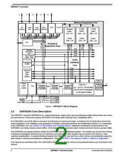
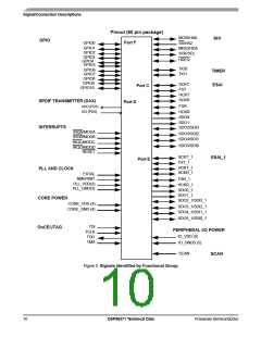
All internal buses on the DSP56300 family members are 24-bit buses. See Figure 1.
2.4.5
Direct Memory Access (DMA)
The DMA block has the following features:
•
•
•
•
Six DMA channels supporting internal and external accesses
One-, two- and three-dimensional transfers (including circular buffering)
End-of-block-transfer interrupts
Triggering from interrupt lines and all peripherals
2.4.6
PLL-based Clock Oscillator
The clock generator in the DSP56300 core is composed of two main blocks: the PLL, which performs clock input division,
frequency multiplication, skew elimination and the clock generator (CLKGEN), which performs low-power division and clock pulse
generation. PLL-based clocking:
•
•
•
Allows change of low-power divide factor (DF) without loss of lock
Provides output clock with skew elimination
Provides a wide range of frequency multiplications (1 to 255), predivider factors (1 to 31), PLL feedback multiplier (2 or
4), Output divide factor (1, 2 or 4) and a power-saving clock divider (2i: i = 0 to 7) to reduce clock noise
The PLL allows the processor to operate at a high internal clock frequency using a low frequency clock input. This feature offers
two immediate benefits:
•
•
A lower frequency clock input reduces the overall electromagnetic interference generated by a system.
The ability to oscillate at different frequencies reduces costs by eliminating the need to add additional oscillators to a
system.
NOTE
The PLL will momentarily overshoot the target frequency when the PLL is first enabled or
when the VCO frequency is modified. It is important that when modifying the PLL frequency
or enabling the PLL that the two step procedure defined in Section 3, DSP56371 Overview
be followed.
2.4.7
On-Chip Memory
The memory space of the DSP56300 core is partitioned into program memory space, X data memory space and Y data memory
space. The data memory space is divided into X and Y data memory in order to work with the two Address ALUs and to feed two
operands simultaneously to the Data ALU. Memory space includes internal RAM and ROM and can not be expanded off-chip.
There is an instruction patch module. The patch module is used to patch program ROM. The memory switch mode is used to
increase the size of program RAM as needed (switch from X data RAM and/or Y data RAM).
6
DSP56371 Technical Data
Freescale Semiconductor

 FREESCALE [ Freescale ]