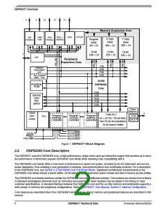
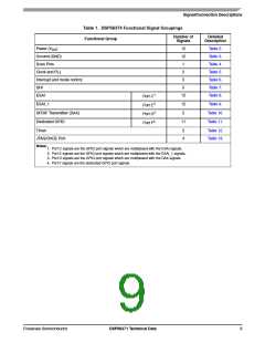
DSP56371 Overview
•
•
•
•
•
•
Program control unit (PCU)
DMA controller (with six channels)
Instruction patch controller
PLL-based clock oscillator
OnCE module
Memory
In addition, the DSP56371 provides a set of on-chip peripherals, described in Section 2.5 Peripheral Overview.
2.4.1 Data ALU
The Data ALU performs all the arithmetic and logical operations on data operands in the DSP56300 core. The components of
the Data ALU are as follows:
•
•
•
•
•
•
Fully pipelined 24-bit × 24-bit parallel multiplier-accumulator (MAC)
Bit field unit, comprising a 56-bit parallel barrel shifter (fast shift and normalization; bit stream generation and parsing)
Conditional ALU instructions
24-bit or 16-bit arithmetic support under software control
Four 24-bit input general purpose registers: X1, X0, Y1 and Y0
Six Data ALU registers (A2, A1, A0, B2, B1 and B0) that are concatenated into two general purpose, 56-bit accumulators
(A and B), accumulator shifters
•
Two data bus shifter/limiter circuits
2.4.1.1
Data ALU Registers
The Data ALU registers can be read or written over the X memory data bus (XDB) and the Y memory data bus (YDB) as 24- or
48-bit operands (or as 16- or 32-bit operands in 16-bit arithmetic mode). The source operands for the Data ALU, which can be
24, 48, or 56 bits (16, 32, or 40 bits in 16-bit arithmetic mode), always originate from Data ALU registers. The results of all Data
ALU operations are stored in an accumulator.
All the Data ALU operations are performed in two clock cycles in pipeline fashion so that a new instruction can be initiated in
every clock, yielding an effective execution rate of one instruction per clock cycle. The destination of every arithmetic operation
can be used as a source operand for the immediately following arithmetic operation without a time penalty (i.e., without a pipeline
stall).
2.4.1.2
Multiplier-Accumulator (MAC)
The MAC unit comprises the main arithmetic processing unit of the DSP56300 core and performs all of the calculations on data
operands. In the case of arithmetic instructions, the unit accepts as many as three input operands and outputs one 56-bit result
of the following form- Extension:Most Significant Product:Least Significant Product (EXT:MSP:LSP).
The multiplier executes 24-bit × 24-bit, parallel, fractional multiplies, between two’s-complement signed, unsigned, or mixed
operands. The 48-bit product is right-justified and added to the 56-bit contents of either the A or B accumulator. A 56-bit result
can be stored as a 24-bit operand. The LSP can either be truncated or rounded into the MSP. Rounding is performed if specified.
4
DSP56371 Technical Data
Freescale Semiconductor

 FREESCALE [ Freescale ]