GPIO Timing
17
GPIO Timing
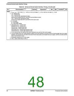
Table 25. GPIO Timing
Characteristics1
No.
Expression
Min
—
Max
7
Unit
ns
ns
ns
ns
ns
ns
ns
ns
ns
ns
106 FOSC edge to GPIO out valid (GPIO out delay time)
107 FOSC edge to GPIO out not valid (GPIO out hold time)
108 FOSC In valid to EXTAL edge (GPIO in set-up time)
109 FOSC edge to GPIO in not valid (GPIO in hold time)
110 Minimum GPIO pulse high width (except Port F)
111 Minimum GPIO pulse low width (except Port F)
112 Minimum GPIO pulse low width (Port F)
113 Minimum GPIO pulse high width (Port F)
114 GPIO out rise time
----
2
7
---
---
—
0
2 x TC
2 x TC
6 x TC
6 x TC
—
11.1
11.1
33.3
33.3
—
13
13
115 GPIO out fall time
—
—
Note:
1. VCORE_VDD = 1.25 V 0.05 V; T = –40°C to 115°C for 150 MHz; T = 0°C to 100°C for 181 MHz; CL = 50 pF
J
J
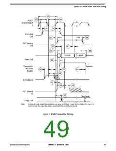
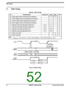
FOSC
106
107
GPIO
(Output)
108
109
GPIO
(Input)
Valid
GPIO
(Output)
110
112
111
113
Figure 20. GPIO Timing
52
DSP56371 Technical Data
Freescale Semiconductor

 FREESCALE [ Freescale ]