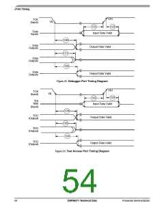
JTAG Timing
18
JTAG Timing
Table 26. JTAG Timing
Characteristics
All frequencies
No.
Unit
Min
0.0
Max
22.0
—
116 TCK frequency of operation (1/(TC × 6); maximum 22 MHz)
117 TCK cycle time
MHz
ns
ns
ns
ns
ns
ns
ns
ns
ns
45.0
20.0
0.0
118 TCK clock pulse width
—
119 TCK rise and fall times
10.0
40.0
40.0
—
120 TCK low to output data valid
121 TCK low to output high impedance
122 TMS, TDI data setup time
123 TMS, TDI data hold time
124 TCK low to TDO data valid
125 TCK low to TDO high impedance
Note:
0.0
0.0
5.0
25.0
0.0
—
44.0
44.0
0.0
1. VCORE_VDD = 1.25 V 0.05 V; TJ = –40°C to 115°C for 150 MHz; TJ = 0°C to 100°C for 181 MHz; CL = 50 pF
All timings apply to OnCE module data transfers because it uses the JTAG port as an interface.
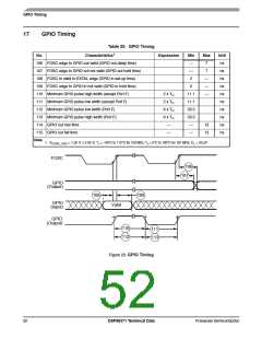
117
118
118
VM
VM
VIH
TCK
(Input)
VIL
119
119
Figure 21. Test Clock Input Timing Diagram
Freescale Semiconductor
DSP56371 Technical Data
53

 FREESCALE [ Freescale ]