Freescale Semiconductor, Inc.
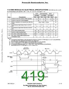
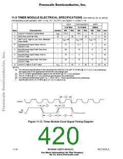
11.10 SERIAL MODULE ELECTRICAL SPECIFICATIONS (See notes (a), (b), (c), and
(d) corresponding to part operation, GND = 0 Vdc, TA = 0 to 70°C; see numbered notes; see Figures 11-15–11-18)
3.3 V or
5.0 V
3.3 V
5.0 V
8.39 MHz
16.78 MHz
25.16 MHz
Num.
Characteristic
CLKOUT Cycle Time
Symbol
Min
119.2
—
Max
Min
59.6
—
Max
—
Min
40
—
5
Max
—
Unit
ns
1
2
t
—
20
—
cyc
Clock Rise or Fall Time
t
10
5
ns
rf
2
3
Clock Input (X1 or SCLK ) Synchronizer Setup
Time
t
t
15
8, 5
—
—
ns
CS
4
Clock Input (X1 or SCLK ) Synchronizer Hold
Time
30
—
15
—
8
—
ns
CH
5
6
7
8
TxD Data Valid from CLKOUT High
X1 Cycle Time
t
0.5 t
Max
Min
Min
Min
VLD
cyc
t
2.25 t
cyc
X1
X1 High or Low Time
t
0.55 t
+ 0.75(t
CS
+ t
)
CH
X1HL
cyc
SCLK High or Low Time, Asynchronous (16x)
Mode
t
t
+ t
+ t
CS CH
AHL
cyc
1
9
SCLK High Time, Synchronous (1x) Mode
SCLK Low Time, Synchronous (1x) Mode
t
t
(Gx) + t (Gx) + t (Gx)
CS CH
Min
Min
SH
cyc
10
t
greater of
SL
({1.5t
0.5t
cyc
(Tx) + t
(Tx) + t
VLD
(Rx) + t (Rx)})
(Tx)} +
cyc
CS
(Rx) + t
CS
or
CH
t
SH
11
12
TxD Data Valid from SCLK Low, Synchronous
(1x) Mode
t
1.5t
(Tx) +
Max
Min
Min
T × D
R × S
R × H
cyc
t
(Tx) + t
(Tx)
CS
VLD
RxD Setup Time to SCLK High, Synchronous
(1x) Mode
t
t
0.5t
0.5t
(Rx) + t
(Rx) + t
(Rx) + t
(Rx) + t
(Rx)
(Rx)
cyc
CS
CS
CH
CH
13
RxD Hold Time from SCLK High, Synchronous
(1x) Mode
cyc
NOTES:
(a) The electrical specifications in this document for both the 8.39 and 16.78 MHz @ 3.3 V ±0.3 V are preliminary
and apply only to the appropriate MC68340V low voltage part.
(b) The 16.78-MHz specifications apply to the MC68340 @ 5.0 V ±5% operation.
(c) The 25.16 MHz @ 5.0 V ±5% electrical specifications are preliminary.
(d) For extended temperature parts T = –40 to +85°C. These specifications are preliminary.
A
1. Asynchronous operation numbers take into account a receiver and transmitter operating at different clock
frequencies. (Rx) refers to receiver value. (Tx) refers to transmitter value. (Gx) refers to the value that is greater,
either receiver or transmitter.
2. Specification #3 for 16.78 MHz @ 3.3 V ±0.3 V will be 8 ns.
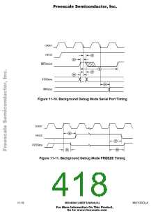
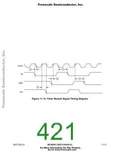
1
CLKOUT
5
TxD
Figure 11-15. Serial Module General Timing Diagram
11-22
MC68340 USER’S MANUAL
MOTOROLA
For More Information On This Product,
Go to: www.freescale.com

 FREESCALE [ Freescale ]