Freescale Semiconductor, Inc.
11.11 IEEE 1149.1 ELECTRICAL SPECIFICATIONS (See notes (a), (b), (c), and (d)
corresponding to part operation, GND = 0 Vdc, TA = 0 to 70°C; see Figures 11-19–11-21)
3.3 V or
5.0 V
3.3 V
5.0 V
8.39 MHz
16.78 MHz
25.16 MHz
Num.
Characteristic
TCK Frequency of Operation
Min
Max
Min
Max
Min
Max
25
Unit
MHz
ns
0
119.2
56
0
8.39
—
0
59.6
28
0
16.78
—
0
1
TCK Cycle Time in Crystal Mode
TCK Clock Pulse Width Measured at 1.5 V
TCK Rise and Fall Times
40
18
0
—
—
3
2
—
—
ns
3
10
—
5
ns
6
Boundary Scan Input Data Setup Time
Boundary Scan Input Data Hold Time
TCK Low to Output Data Valid
TCK Low to Output High Impedance
TMS, TDI Data Setup Time
32
52
0
16
26
0
—
10
18
0
—
—
26
40
—
—
16
16
ns
7
—
—
ns
8
9
80
120
—
40
60
—
ns
0
0
0
ns
10
30
30
0
15
15
0
10
10
0
ns
11
TMS, TDI Data Hold Time
—
—
ns
12
TCK Low to TDO Data Valid
50
50
25
25
ns
13
TCK Low to TDO High Impedance
0
0
0
ns
NOTES:
(a) The electrical specifications in this document for both the 8.39 and 16.78 MHz @ 3.3 V ±0.3 V are preliminary,
and apply only to the appropriate MC68340V low voltage part.
(b) The 16.78-MHz specifications apply to the MC68340 @ 5.0 V ±5% operation.
(c) The 25.16 MHz @ 5.0 V ±5% electrical specifications are preliminary.
(d) For extended temperature parts T = –40 to +85°C. These specifications are preliminary.
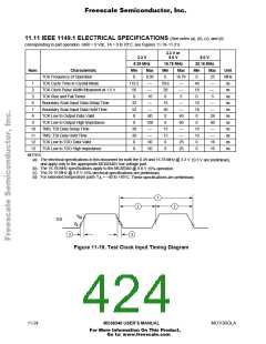
A
1
2
2
V
IH
TCK
V
IL
3
3
Figure 11-19. Test Clock Input Timing Diagram
11-24
MC68340 USER’S MANUAL
MOTOROLA
For More Information On This Product,
Go to: www.freescale.com

 FREESCALE [ Freescale ]