Freescale Semiconductor, Inc.
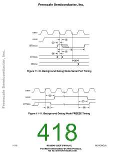
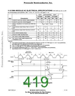
11.8 DMA MODULE AC ELECTRICAL SPECIFICATIONS (See notes (a), (b), (c), and
(d) corresponding to part operation, GND = 0 Vdc, TA = 0 to 70°C; see Figure 11-12)
3.3 V
3.3 V or 5.0 V
16.78 MHz
5.0 V
8.39 MHz
25.16 MHz
Num.
Characteristic
Min
—
Max
Min
—
Max
30
Min
—
Max
20
Unit
ns
1
2
3
CLKOUT Low to AS, DACK, DONE Asserted
CLKOUT Low to AS, DACK Negated
60
60
—
—
30
—
20
ns
DREQ≈ Asserted to AS Asserted (for DMA Bus
3t
+ t
+ t
ns
cyc AIST CLSA
Cycle)
1
4
Asynchronous Input Setup Time to CLKOUT
Low
15
30
—
—
8, 5
15
—
—
5
—
—
ns
ns
5
Asynchronous Input Hold Time from CLKOUT
Low
10
6
7
AS to DACK Assertion Skew
DACK to DONE Assertion Skew
AS, DACK, DONE Width Asserted
-30
-30
200
80
30
30
—
—
–15
–15
100
40
15
15
—
—
–10
–8
10
8
ns
ns
ns
ns
8
70
—
—
8A
AS, DACK, DONE Width Asserted (Fast
Termination Cycle)
28
NOTES:
(a) The electrical specifications in this document for both the 8.39 and 16.78 MHz @ 3.3 V ±0.3 V are preliminary
and apply only to the appropriate MC68340V low voltage part.
(b) The 16.78-MHz specifications apply to the MC68340 @ 5.0 V ±5% operation.
(c) The 25.16 MHz @ 5.0 V ±5% electrical specifications are preliminary.
(d) For extended temperature parts T = –40 to +85°C. These specifications are preliminary.
A
1. Specification #4 for 16.78 MHz @ 3.3 V ±0.3 V will be 8 ns.
CPU_CYCLE
(DMA REQUEST)
DMA_CYCLE
S2
S0
S1
S2
S4
S5
S0
S1
1
S4
S5
S3
S3
CLKOUT
4
5
DONE (INPUT)
DREQ
6
3
8
AS
1
2
DACK
7
DONE
(OUTPUT)
1
Figure 11-12. DMA Signal Timing Diagram
MOTOROLA
MC68340 USER’S MANUAL
11-19
For More Information On This Product,
Go to: www.freescale.com

 FREESCALE [ Freescale ]