Freescale Semiconductor, Inc.
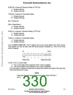
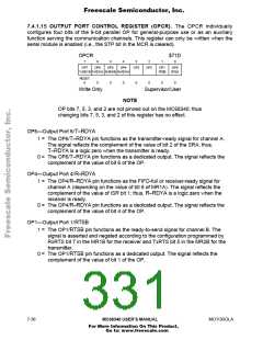
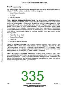
7.4.1.15 OUTPUT PORT CONTROL REGISTER (OPCR). The OPCR individually
configures four bits of the 8-bit parallel OP for general-purpose use or as an auxiliary
function serving the communication channels. This register can only be written when the
serial module is enabled (i.e., the STP bit in the MCR is cleared).
OPCR
$71D
7
6
5
4
3
2
1
0
OP7
OP6
OP5
OP4
OP3
OP2
OP1
OP0
T≈RDYB T≈RDYA R≈RDYB R≈RDYA
RTSB
RTSA
RESET:
0
0
0
0
0
0
0
0
Write Only
Supervisor/User
NOTE
OP bits 7, 5, 3, and 2 are not pinned out on the MC68340; thus
changing bits 7, 5, 3, and 2 of this register has no effect.
OP6—Output Port 6/T≈RDYA
1 = The OP6/T≈RDYA pin functions as the transmitter-ready signal for channel A.
The signal reflects the complement of the value of bit 2 of the SRA; thus,
T≈RDYA is a logic zero when the transmitter is ready.
0 = The OP6/T≈RDYA pin functions as a dedicated output. The signal reflects the
complement of the value of bit 6 of the OP.
OP4—Output Port 4/R≈RDYA
1 = The OP4/R≈RDYA pin functions as the FIFO-full or receiver-ready signal for
channel A (depending on the value of bit 6 of MR1A). The signal reflects the
complement of the value of ISR bit 1; thus, R≈RDYA is a logic zero when the
receiver is ready.
0 = The OP4/R≈RDYA pin functions as a dedicated output. The signal reflects the
complement of the value of bit 4 of the OP.
OP1—Output Port 1/RTSB
1 = The OP1/RTSB pin functions as the ready-to-send signal for channel B. The
signal is asserted and negated according to the configuration programmed by
RxRTS bit 7 in the MR1B for the receiver and TxRTS bit 5 in the MR2B for the
transmitter.
0 = The OP1/RTSB pin functions as a dedicated output. The signal reflects the
complement of the value of bit 1 of the OP.
7- 36
MC68340 USER’S MANUAL
MOTOROLA
For More Information On This Product,
Go to: www.freescale.com

 FREESCALE [ Freescale ]