Freescale Semiconductor, Inc.
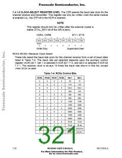
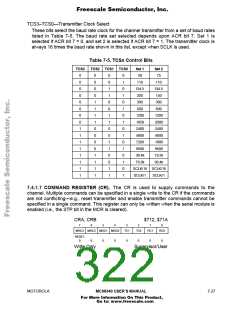
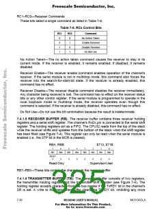
RC1–RC0—Receiver Commands
These bits select a single command as listed in Table 7-8.
Table 7-8. RCx Control Bits
RC1
0
RC0
0
Command
No Action Taken
Enable Receiver
Disable Receiver
Do Not Use
0
1
1
0
1
1
No Action Taken—The no action taken command causes the receiver to stay in its
current mode. If the receiver is enabled, it remains enabled; if disabled, it remains
disabled.
Receiver Enable—The receiver enable command enables operation of the channel's
receiver. If the serial module is not in multidrop mode, this command also forces the
receiver into the search-for-start-bit state. If the receiver is already enabled, this
command has no effect.
Receiver Disable—The receiver disable command disables the receiver immediately.
Any character being received is lost. The command has no effect on the receiver status
bits or any other control register. If the serial module is programmed to operate in the
local loopback mode or multidrop mode, the receiver operates even though this
command is selected. If the receiver is already disabled, this command has no effect.
Do Not Use—Do not use this bit combination because the result is indeterminate.
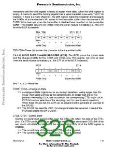
7.4.1.8 RECEIVER BUFFER (RB). The receiver buffer contains three receiver holding
registers and a serial shift register. The channel's RxDx pin is connected to the serial shift
register. The holding registers act as a FIFO. The CPU32 reads from the top of the stack
while the receiver shifts and updates from the bottom of the stack when the shift register
has been filled (see Figure 7-4). This register can only be read when the serial module is
enabled (i.e., the STP bit in the MCR is cleared).
RBA, RBB
$713, $71B
7
6
5
4
3
2
1
0
RB7
RB6
RB5
RB4
RB3
RB2
RB1
RB0
RESET:
0
0
0
0
0
0
0
0
Read Only
Supervisor/User
RB7–RB0—These bits contain the character in the receiver buffer.
7.4.1.9 TRANSMITTER BUFFER (TB). The transmitter buffer consists of two registers,
the transmitter holding register and the transmitter shift register (see Figure 7-4). The
holding register accepts characters from the bus master if the TxRDY bit in the channel's
SR is set. A write to the transmitter buffer clears the TxRDY bit, inhibiting any more
7- 30
MC68340 USER’S MANUAL
MOTOROLA
For More Information On This Product,
Go to: www.freescale.com

 FREESCALE [ Freescale ]