Freescale Semiconductor, Inc.
Multiple Serial Interface
Serial Peripheral Interface (SPI)
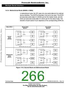
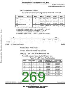
SPC0 — Serial Pin Control 0
This bit decides serial pin configurations with MSTR control bit.
SPC0(1)
MISO(2)
MOSI(3)
SCK(4)
SS(5)
SS In
Pin Mode
MSTR
#1
#2
#3
#4
0
1
0
1
Slave Out
Slave In
SCK In
Normal
0
Master In Master Out SCK Out
SS I/O
SS In
SS I/O
Slave I/O
GPI/O
GPI/O
SCK In
Bidirectional
1
Master I/O SCK Out
1. The serial pin control 0 bit enables bidirectional configurations.
2. Slave output is enabled if DDS4 = 1, SS = 0 and MSTR = 0. (#1, #3)
3. Master output is enabled if DDS5 = 1 and MSTR = 1. (#2, #4)
4. SCK output is enabled if DDS6 = 1 and MSTR = 1. (#2, #4)
5. SS output is enabled if DDS7 = 1, SSOE = 1 and MSTR = 1. (#2, #4)
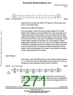
Bit 7
6
0
0
5
0
0
4
0
0
3
0
0
2
SPR2
0
1
SPR1
0
Bit 0
SPR0
0
0
0
RESET:
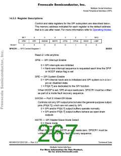
SP0BR — SPI Baud Rate Register
$00D2
Read anytime. Write anytime.
At reset, E Clock divided by 2 is selected.
SPR[2:0] — SPI Clock (SCK) Rate Select Bits
These bits are used to specify the SPI clock rate.
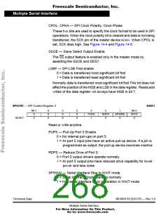
Table 14-4. SPI Clock Rate Selection
E Clock
Divisor
Frequency at
E Clock = 4 MHz E Clock = 8 MHz
Frequency at
SPR2 SPR1 SPR0
0
0
0
0
1
1
1
1
0
0
1
1
0
0
1
1
0
1
0
1
0
1
0
1
2
4
2.0 MHz
1.0 MHz
500 kHz
250 kHz
125 kHz
62.5 kHz
31.3 kHz
15.6 kHz
4.0 MHz
2.0 MHz
1.0 MHz
500 KHz
250 KHz
125 KHz
62.5 KHz
31.3 KHz
8
16
32
64
128
256
MC68HC912DG128 — Rev 3.0
Technical Data
Multiple Serial Interface
For More Information On This Product,
Go to: www.freescale.com

 FREESCALE [ Freescale ]