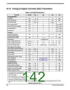
Equivalent Circuit for ADC Inputs
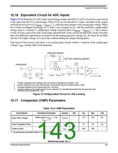
10.16 Equivalent Circuit for ADC Inputs
Figure 10-18 illustrates the ADC input circuit during sample and hold. S1 and S2 are always open/closed
at the same time that S3 is closed/open. When S1/S2 are closed and S3 is open, one input of the sample
and hold circuit moves to (V
- V
) / 2, while the other charges to the analog input voltage. When
REFHx
REFLx
the switches are flipped, the charge on C1 and C2 are averaged via S3, with the result that a single-ended
analog input is switched to a differential voltage centered about (V - V ) / 2. The switches
REFHx
REFLx
switch on every cycle of the ADC clock (open one-half ADC clock, closed one-half ADC clock). Note that
there are additional capacitances associated with the analog input pad, routing, etc., but these do not filter
into the S/H output voltage, as S1 provides isolation during the charge-sharing phase.
One aspect of this circuit is that there is an on-going input current, which is a function of the analog input
voltage, V , and the ADC clock frequency.
REF
125Ω ESD Resistor
8pF noise damping capacitor
4
3
Analog Input
S1
C1
S/H
S3
C2
S2
(VREFHx - VREFLx ) / 2
2
1
C1 = C2 = 1pF
1. Parasitic capacitance due to package, pin-to-pin and pin-to-package base coupling; 1.8pF
2. Parasitic capacitance due to the chip bond pad, ESD protection devices and signal routing; 2.04pF
3. Equivalent resistance for the channel select mux; 100 ohms
4. Sampling capacitor at the sample and hold circuit. Capacitor C1 is normally disconnected from the input and is only
connected to it at sampling time; 1.4pF
Figure 10-18 Equivalent Circuit for A/D Loading
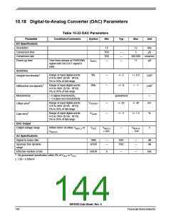
10.17 Comparator (CMP) Parameters
Table 10-21 CMP Parameters
Characteristic
Conditions/Comments
Symbol
Min
Typ
Max
Unit
Input Offset Voltage1
Within range of VDDA - .1V to
VSSA + .1V
VOFFSET
—
±10
±35
mV
Input Propagation Delay
Power-up time
tPD
—
—
35
45
ns
tCPU
TBD
TBD
1. No guaranteed specification within 0.1V of V
or V
SSA
DDA
56F8036 Data Sheet, Rev. 6
Freescale Semiconductor
143

 FREESCALE [ Freescale ]