F71872
7.7.3.2 Command register
The internal KBC operation is controlled by the KBC command byte (KCCB). The KCCB resides in I/O address 64h
that is read with a 20h command and written with a 60h command data.
Bit
7
Name
Reserved
R/W Default
Description
-
-
Reserved
6
Translate code
R/W
1
0: Pass un-translated scan code.
1: Translate scan code to IBM PC standard.
5
Disable Auxiliary
Device
R/W
0
1: Disable Auxiliary inhibit function.
4
3
2
Disable Keyboard R/W
0
-
1: Disable keyboard inhibit function.
Reserved
Reserved
-
System flag
R/W
1
0: The system is executing POST as a result of a cold boot.
1: The system is executing POST as a result of a shutdown or warm boot.
1
0
Enable Auxiliary
Interrupt
R/W
R/W
1
1
0: Ao interrupt
1: A system interrupt is generated when a byte is placed in output buffer
(IRQ12).
Enable keyboard
Interrupt
0:No interrupt
1: A system interrupt is generated when a byte is placed in output buffer
(IRQ1).
7.7.3.3 DATA register
The DATA register is an 8 bits register at I/O address 60h. the KBC used the output buffer to send the scan code
received from keyboard and data byte replay by command to the system.
Power on default <7:0> = 00000000 binary
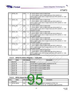
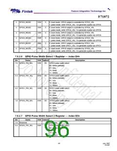
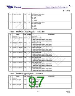
7.8 GPIO Registers
7.8.1 Logic Device Number Register
Logic Device Number Register Index 07H
Bit
Name
R/W Default
Description
91
July, 2007
V0.28P

 FINTEK [ FEATURE INTEGRATION TECHNOLOGY INC. ]