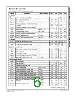
Electrical Characteristics
VDD = 15V and TA = 25°C unless otherwise noted.
Symbol
Parameter
Test Condition
Min.
Typ.
Max. Unit
VDD Section
VDD-OP
Continuously Operating Voltage
Turn-on Threshold Voltage
Turn-off Voltage
20
V
V
V
VDD-ON
15.5
9.5
16.5
10.5
17.5
11.5
VDD-OFF
Threshold voltage on VDD for Short-Circuit
Protection
VDD-OFF VDD-OFF VDD-OFF
+0.5V +1.0V +1.5V
VDD-SCP
V
VDD-LH
IDD-ST
Threshold Voltage for Latch-off Release
Startup Current
3
4
8
5
V
µA
mA
V
VDD-ON – 0.16V
GATE Open
30
IDD-OP
Operating Supply Current
3.7
23.6
100
50
5.0
24.6
140
70
VDD-OVP
tD-VDDOVP
IDD-OVP
VDD Over-Voltage Protection (Latch off)
VDD OVP Debounce Time
22.6
60
RI = 26kꢀ
µs
µA
VDD OVP Latch-off Holding Current
VDD = 5V
30
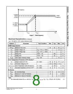
VIN Section
VIN-OFF
PWM Turn-off Threshold Voltage
PWM Turn-on Threshold Voltage
0.65
0.70
0.75
V
V
VIN-OFF VIN-OFF VIN-OFF
+0.18 +0.20 +0.22
VIN-ON
Feedback Input Section
AV
ZFB
Input-Voltage to Current-Sense Attenuation
1/3.5
4.0
1/4.0
5.5
1/4.5
7.0
V/V
kꢀ
V
Input Impedance
VFBO
VFB-OLP
tD-OLP
FB Pin Open Voltage
5.2
6.2
6.6
Threshold Voltage of Open-loop Protection
Open-loop Protection Delay Time
4.7
5.2
5.7
V
RI = 26kꢀ
1600
1700
1800
ms
Current Sense Section
ZSENSE Input Impedance
tPD
12
kꢀ
ns
ns
V
Delay to Output
100
250
tLEB
Leading-edge Blanking Time
270
0.30
0.80
0.67
0.58
0.48
1600
360
VSLOPE
VSTH1V
VSTH3V
VSTH1V-2/3
VSTH3V-2/3
tD-OCP
Slope Compensation
Duty = DCYMAX
VIN = 1V
0.33
0.83
0.70
0.61
0.51
1700
0.36
0.86
0.73
0.64
0.54
1800
Threshold Voltage for Current Limit
Threshold Voltage for Current Limit
OCP Threshold Voltage for Current Limit
OCP Threshold Voltage for Current Limit
Delay Time for Over-Current Protection
V
VIN = 3V
V
VIN = 1V
V
VIN = 3V
V
RI = 26kꢀ
ms
Delay Time for Output Short-Circuited
Protection
RI = 26kꢀ;
tD-SCP
90
100
110
ms
VDD<VDD-SCP
tSS-65KHz
RI = 26kꢀ
RI = 13kꢀ
4.5
5.0
5.5
ms
ms
Period During Startup Time
tSS-130KHz
2.25
2.50
2.75
Continued on following page…
© 2008 Fairchild Semiconductor Corporation
SG6846A • Rev. 1.1.4
www.fairchildsemi.com
6

 FAIRCHILD [ FAIRCHILD SEMICONDUCTOR ]