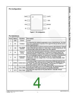
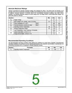
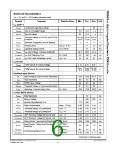
Pin Configuration
Figure 5. Pin Configuration
Pin Definitions
Pin # Name
Function
Description
1
GND
Ground
Ground.
The signal from the external compensation circuit is fed into this pin. The PWM
duty cycle is determined in response to the signal from this pin and the current-
sense signal from pin 6.
2
FB
Feedback
Line-voltage detection is used for brownout protection with hysteresis. Constant
output power limit over universal AC input range is achieved using this pin. Add
a low-pass filter to filter out line ripple on the bulk capacitor.
Line-voltage
Detection
3
4
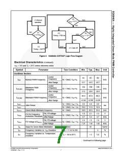
VIN
RI
A resistor from the RI pin to ground generates a reference current source that
determines the switching frequency. Increasing the resistance reduces the
switching frequency. A 26kΩ resistor results in a 65kHz switching frequency.
Reference
Setting
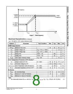
For over-temperature protection, an external NTC thermistor is connected from
Temperature this pin to the GND pin. The impedance of the NTC decreases at high
5
6
RT
Detection
temperatures. Once the voltage of the RT pin drops below a threshold, PWM
output is disabled.
The sensed voltage is used for peak-current-mode control and cycle-by-cycle
current limiting. If the switching current is higher than OCP threshold and lasts
for 1700ms, SG6846A turns off immediately. This two-level OCP feature is
especially suitable for SMPS with surge current output.
SENSE Current Sense
If an open-circuit failure occurs in the feedback loop, the internal protection
circuit disables PWM output as long as VDD exceeds a threshold.
7
8
VDD
Power Supply
Driver Output
The totem-pole output driver for the power MOSFET; internally clamped
below 18V.
GATE
© 2008 Fairchild Semiconductor Corporation
SG6846A • Rev. 1.1.4
www.fairchildsemi.com
4

 FAIRCHILD [ FAIRCHILD SEMICONDUCTOR ]