P-CHANNEL
POWER MOSFET
SFP9634
Electrical Characteristics (TC=25oC unless otherwise specified)
Symbol
BVDSS
Characteristic
Min. Typ. Max. Units
Test Condition
VGS=0V,ID=-250mA
Drain-Source Breakdown Voltage
Breakdown Voltage Temp. Coeff.
Gate Threshold Voltage
V
V/oC
V
-250 --
-- -0.22 --
-2.0 -- -4.0
-- -100
--
DBV/DTJ
VGS(th)
ID=-250mA
DS=-5V,ID=-250mA
VGS=-30V
GS=30V
VDS=-250V
DS=-200V,TC=125oC
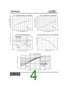
See Fig 7
V
Gate-Source Leakage , Forward
Gate-Source Leakage , Reverse
--
--
--
--
IGSS
nA
V
--
--
100
-10
IDSS
Drain-to-Source Leakage Current
mA
V
-- -100
Static Drain-Source
On-State Resistance
Forward Transconductance
Input Capacitance
4
RDS(on)
VGS=-10V,ID=-2.5A
VDS=-40V,ID=-2.5A
--
--
W
W
1.3
O
gfs
Ciss
Coss
Crss
td(on)
tr
4
--
--
--
--
--
--
--
--
--
--
--
3.6
--
O
750 975
VGS=0V,VDS=-25V,f =1MHz
Output Capacitance
Reverse Transfer Capacitance
Turn-On Delay Time
Rise Time
165
65
35
50
90
40
37
--
110
45
pF
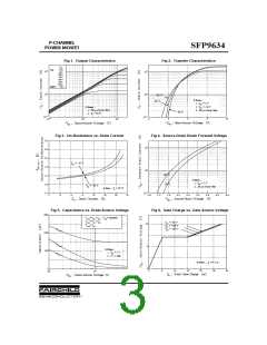
See Fig 5
13
VDD=-125V,ID=-5.0A,
20
RG=12 W
ns
td(off)
tf
Turn-Off Delay Time
Fall Time
40
4
See Fig 13
5
O O
16
Qg
Total Gate Charge
Gate-Source Charge
Gate-Drain( “ Miller “ ) Charge
29
V
DS=-200V,VGS=-10V,
Qgs
Qgd
nC
5.4
15.5
ID=-5.0A
4
5
--
See Fig 6 & Fig 12
OO
Source-Drain Diode Ratings and Characteristics
Symbol
Characteristic
Continuous Source Current
Pulsed-Source Current
Diode Forward Voltage
Reverse Recovery Time
Reverse Recovery Charge
Min. Typ. Max. Units
Test Condition
Integral reverse pn-diode
in the MOSFET
TJ=25oC,IS=-5.0A,VGS=0V
TJ=25oC,IF=-5.0A
IS
ISM
VSD
trr
--
--
--
--
-- -5.0
-- -20
-- -5.0
170 --
A
1
O
V
4
O
ns
mC
Qrr
4
O
-- 1.17 --
diF/dt=100A/ms
Notes ;
Repetitive Rating : Pulse Width Limited by Maximum Junction Temperature
1
O
L=20mH, IAS=-5.0A, VDD=-50V, RG=27W*, Starting TJ =25oC
2
O
BVDSS , Starting TJ =25oC
_
_
<
_
3
I
-5.0A, di/dt 400A/ms, V
<
<
O
SD
DD
_
4
Pulse Test : Pulse Width = 250 ms, Duty Cycle <2%
O
Essentially Independent of Operating Temperature
5
O

 FAIRCHILD [ FAIRCHILD SEMICONDUCTOR ]