RC4200
PRODUCT SPECIFICATION
Inputs
VZ
+VS
VOS4 ADJ
R1
8
7
VX
R4
100 R4
I
1
5
R
s
C
s
+V
I
S
4
-VS
VOS1
50 mV
RC4200
Multiplier
R1
100
RO
0.1 µF
50 mV
R2
-VS
1
VY
I
2
Gain
Adj.
R
s
4
C
s
+V
Output
VO
S
1/4
4156
I
3
VOS3
VOS2
2
µ
F
0.1
3
6
100
µ
0.1
F
50 mV
-VS
+V
S
-VS
R O
µ
RS = 10K, CS = 0.005
VX VY
F
µ
100 V
-VS
V
=
K
s
V
z
65-1867
RO R4
R1 R2
Where K =
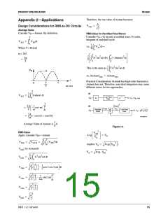
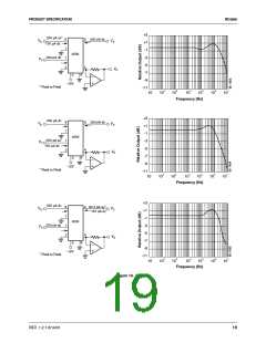
Limited Range, First Quadrant Applications
Thermal Symmetry
The following circuit has the advantage that cross-product
errors are due only to input offsets and nonlinearity error is
sightly error is slightly less for lower input currents.
I
1
2
3
4
8
7
6
5
I
1
2
V
V
The circuit also has no standby current to add to the noise
content, although the signal-to-noise ratio worsens at very
low input currents (1-5 µA) due to the noise current of the
input stages.
Thermal
Symmetry
Line
OS2
–V
OS1
GND
S
Output I
I
4
3
The R C filter circuits are added to each input to improve
S S
the stability for input currents below 50 µA.
65-0070
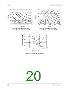
The scale factor is sensitive to temperature gradients across
the chip in the lateral direction. Where possible, the package
should be oriented such that forces generating temperature
gradients are located physically on the line of thermal sym-
metry. This will minimize scale-factor error due to thermal
gradients.
Caution!
The bandpass drops off significantly for lower currents
(<50 µA) and non-symmetrical rise and fall times can cause
second harmonic distortion.
18
REV. 1.2.1 6/14/01

 FAIRCHILD [ FAIRCHILD SEMICONDUCTOR ]