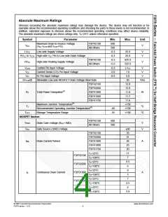
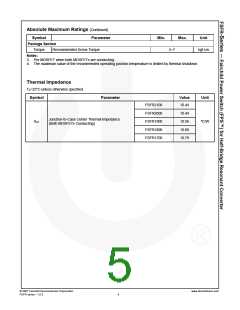
Absolute Maximum Ratings
Stresses exceeding the absolute maximum ratings may damage the device. The device may not function or be
operable above the recommended operating conditions and stressing the parts to these levels is not recommended. In
addition, extended exposure to stresses above the recommended operating conditions may affect device reliability.
The absolute maximum ratings are stress ratings only. TA=25°C unless otherwise specified.
Symbol
VDS
Parameter
Min.
600
500
-0.3
-0.3
-0.3
-0.3
-0.3
-5.0
-0.3
Max.
Unit
Maximum Drain-to-Source Voltage
(VDL-VCTR and VCTR-PG)
FSFR2100
All Others
V
LVCC
Low-side Supply Voltage
25.0
25.0
625.0
525.0
LVCC
1.0
V
V
HVCC to VCTR High-side VCC Pin to Low-side Drain Voltage
FSFR2100
All Others
HVCC
High-side Floating Supply Voltage
V
VCON
VCS
Control Pin Input Voltage
V
V
Current Sense (CS) Pin Input Voltage
RT Pin Input Voltage
VRT
5.0
V
dVCTR/dt
Allowable Low-side MOSFET Drain Voltage Slew Rate
FSFR2100
50
V/ns
12.0
12.0
11.8
11.7
11.6
+150
+130
+150
FSFR2000
FSFR1900
FSFR1800
FSFR1700
PD
Total Power Dissipation(3)
W
Maximum Junction Temperature(4)
Recommended Operating Junction Temperature(4)
TJ
°C
°C
-40
-55
TSTG
Storage Temperature Range
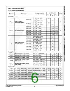
MOSFET Section
FSFR2100
All Others
600
500
VDGR
VGS
V
V
Drain Gate Voltage (RGS=1MΩ)
Gate Source (GND) Voltage
±30
33
31
26
23
20
11
7
FSFR2100
FSFR2000
FSFR1900
FSFR1800
FSFR1700
TC=25°C
IDM
Drain Current Pulsed
A
FSFR2100
FSFR2000
FSFR1900
FSFR1800
FSFR1700
TC=100°C
TC=25°C
9.5
6
TC=100°C
TC=25°C
8
ID
Continuous Drain Current
A
5
TC=100°C
TC=25°C
7
4.5
6
TC=100°C
TC=25°C
3.9
TC=100°C
© 2007 Fairchild Semiconductor Corporation
FSFR series • 1.0.3
www.fairchildsemi.com
4

 FAIRCHILD [ FAIRCHILD SEMICONDUCTOR ]