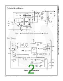
Pin Configuration
1
2
3 4
RT SG LVcc
CON
5
6
7
8
9
10
VCTR
VDL
CS PG
HVcc
Figure 3. Package Diagram
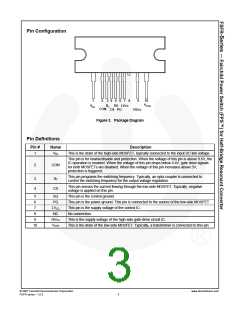
Pin Definitions
Pin #
Name
Description
1
VDL
This is the drain of the high-side MOSFET, typically connected to the input DC link voltage.
This pin is for enable/disable and protection. When the voltage of this pin is above 0.6V, the
IC operation is enabled. When the voltage of this pin drops below 0.4V, gate drive signals
for both MOSFETs are disabled. When the voltage of this pin increases above 5V,
protection is triggered.
2
CON
This pin programs the switching frequency. Typically, an opto-coupler is connected to
control the switching frequency for the output voltage regulation.
3
4
RT
This pin senses the current flowing through the low-side MOSFET. Typically, negative
voltage is applied on this pin.
CS
5
6
SG
PG
This pin is the control ground.
This pin is the power ground. This pin is connected to the source of the low-side MOSFET.
This pin is the supply voltage of the control IC.
7
LVCC
NC
8
No connection.
9
HVCC
VCTR
This is the supply voltage of the high-side gate-drive circuit IC.
This is the drain of the low-side MOSFET. Typically, a transformer is connected to this pin.
10
© 2007 Fairchild Semiconductor Corporation
FSFR series • 1.0.3
www.fairchildsemi.com
3

 FAIRCHILD [ FAIRCHILD SEMICONDUCTOR ]