Electrical Characteristics (TJ = 25°C, Unless Otherwise Specified)
Inverter Part
Symbol
Parameter
Conditions
Min. Typ. Max. Units
VCE(SAT)
Collector-Emitter Saturation VCC = VBS = 15V
IC = 20A, TJ = 25°C
-
-
2.0
V
Voltage
V
IN = 5V
VF
FWD Forward Voltage
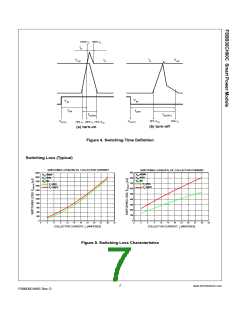
Switching Times
VIN = 0V
IF = 20A, TJ = 25°C
-
-
-
-
-
-
-
-
-
-
-
-
-
2.1
V
μs
μs
μs
μs
μs
μs
μs
μs
μs
μs
mA
HS
tON
tC(ON)
tOFF
tC(OFF)
trr
VPN = 300V, VCC = VBS = 15V
C = 30A
IN = 0V ↔ 5V, Inductive Load
0.75
0.2
0.4
0.1
0.1
0.55
0.35
0.4
0.1
0.1
-
-
-
-
-
-
-
-
-
-
-
1
I
V
(Note 3)
LS
tON
VPN = 300V, VCC = VBS = 15V
I
V
C = 30A
IN = 0V ↔ 5V, Inductive Load
tC(ON)
tOFF
tC(OFF)
trr
(Note 3)
ICES
Collector-Emitter
Leakage Current
VCE = VCES
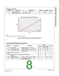
Note:
3.
t
and t
include the propagation delay time of the internal drive IC. t
and t
are the switching time of IGBT itself under the given gate driving condition internally.
C(OFF)
ON
OFF
C(ON)
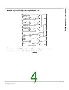
For the detailed information, please see Figure 4.
Control Part
Symbol
Parameter
Conditions
Min.
Typ. Max. Units
IQCCL
IQCCH
IQBS
Quiescent VCC Supply
Current
VCC = 15V
IN(UL, VL, WL) = 0V
VCC(L) - COM
-
-
-
-
23
mA
μA
μA
VCC = 15V
IN(UH, VH, WH) = 0V
VCC(H) - COM
-
-
600
500
Quiescent VBS Supply
Current
VBS = 15V
IN(UH, VH, WH) = 0V
VB(U) - VS(U), VB(V) -VS(V),
VB(W) - VS(W)
VFOH
VFOL
Fault Output Voltage
VSC = 0V, VFO Circuit: 4.7kΩ to 5V Pull-up
VSC = 1V, VFO Circuit: 4.7kΩ to 5V Pull-up
VCC = 15V (Note 4)
4.5
-
-
-
0.8
0.55
-
V
V
-
0.45
-
VSC(ref)
TSD
Short Circuit Trip Level
0.5
160
V
Over-temperature
tion
protec- Temperature at LVIC
°C
ΔTSD
Over-temperature
tion hysterisis
protec- Temperature at LVIC
-
5
-
°C
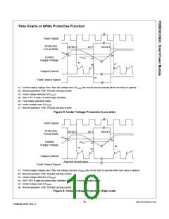
UVCCD
UVCCR
UVBSD
UVBSR
tFOD
Supply Circuit Under-
Voltage Protection
Detection Level
Reset Level
10.7
11.2
10
11.9
12.4
11
13.0
13.4
12
V
V
Detection Level
Reset Level
V
10.5
1.0
2.8
-
11.5
1.8
-
12.5
-
V
Fault-out Pulse Width
ON Threshold Voltage
CFOD = 33nF (Note 5)
ms
V
VIN(ON)
Applied between IN(UH), IN(VH), IN(WH), IN(UL)
IN(VL), IN(WL) - COM
,
-
VIN(OFF) OFF Threshold Voltage
-
0.8
V
Note:
4. Short-circuit current protection is functioning only at the low-sides.
-6
5. The fault-out pulse width t
depends on the capacitance value of C
according to the following approximate equation : C
= 18.3 x 10 x t
[F]
FOD
FOD
FOD
FOD
6
www.fairchildsemi.com
FSBB30CH60C Rev. D

 FAIRCHILD [ FAIRCHILD SEMICONDUCTOR ]