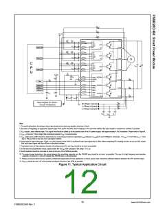
RE(WH)
RE(VH)
15V line
RE(UH)
RBS
DBS
P (27)
(19) VB(W)
(18) VCC(WH)
VB
VCC
COM
IN
OUT
CBS
DBS
CBSC
CBSC
CBSC
(17) IN(WH)
(20) VS(W)
W (26)
Gating WH
Gating VH
VS
RBS
(15) VB(V)
VB
VCC
COM
IN
(14) VCC(VH)
OUT
VS
CBS
(13) IN(VH)
(16) VS(V)
V (25)
U (24)
M
DBS
RBS
(11) VB(U)
VB
VCC
C
P
U
(10) VCC(UH)
CDCS
Vdc
OUT
VS
COM
IN
CBS
(9) IN(UH)
(12) VS(U)
Gating UH
RF
5V line
RPF
(8) CSC
(7) CFOD
(6) VFO
CSC
OUT(WL)
OUT(VL)
C(SC)
C(FOD)
VFO
RSW
NW (23)
NV (22)
NU (21)
RS
CFOD
Fault
(5) IN(WL)
(4) IN(VL)
(3) IN(UL)
Gating WL
Gating VL
Gating UL
IN(WL)
IN(VL)
IN(UL)
RSV
(2) COM
(1) VCC(L)
COM
VCC
CPF
CBPF
OUT(UL)
VSL
RSU
CSPC15
CSP15
RFW
RFV
RFU
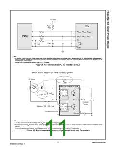
Input Signal for Short-
Circuit Protection
W-Phase Current
V-Phase Current
U-Phase Current
CFW
CFU
CFV
Note:
1. To avoid malfunction, the wiring of each input should be as short as possible. (less than 2-3cm)
2. By virtue of integrating an application specific type HVIC inside the SPM, direct coupling to CPU terminals without any opto-coupler or transformer isolation is possible.
3. V output is open collector type. This signal line should be pulled up to the positive side of the 5V power supply with approximately 4.7kΩ resistance. Please refer to Figure 9.
FO
4. C
of around 7 times larger than bootstrap capacitor C is recommended.
BS
SP15
5. V output pulse width should be determined by connecting an external capacitor(C
FO
) between C
(pin7) and COM(pin2). (Example : if C
= 33 nF, then t = 1.8ms
FOD FO
FOD
FOD
(typ.)) Please refer to the note 5 for calculation method.
6. Input signal is High-Active type. There is a 3.3kΩ resistor inside the IC to pull down each input signal line to GND. When employing RC coupling circuits, set up such RC couple
that input signal agree with turn-off/turn-on threshold voltage.
7. To prevent errors of the protection function, the wiring around R and C should be as short as possible.
F
SC
8. In the short-circuit protection circuit, please select the R C time constant in the range 1.5~2 µs.
F
SC
9. Each capacitor should be mounted as close to the pins of the SPM as possible.
10. To prevent surge destruction, the wiring between the smoothing capacitor and the P&GND pins should be as short as possible. The use of a high frequency non-inductive
capacitor of around 0.1~0.22 µF between the P&GND pins is recommended.
11. Relays are used at almost every systems of electrical equipments of home appliances. In these cases, there should be sufficient distance between the CPU and the relays.
12. C
should be over 1uF and mounted as close to the pins of the SPM as possible.
SPC15
Figure 11. Typical Application Circuit
12
www.fairchildsemi.com
FSBB20CH60 Rev. C

 FAIRCHILD [ FAIRCHILD SEMICONDUCTOR ]