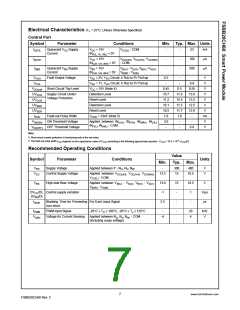
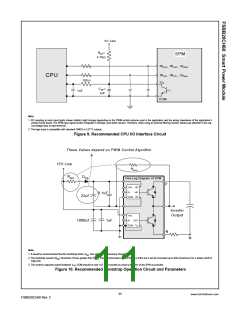
5V-Line
RPF
4.7kΩ
=
SPM
,
,
IN(UH) IN(VH)
IN(WH)
IN(WL)
,
,
IN(UL) IN(VL)
CPU
100 Ω
VFO
CPF
1nF
=
1nF
COM
Note:
1. RC coupling at each input (parts shown dotted) might change depending on the PWM control scheme used in the application and the wiring impedance of the application’s
printed circuit board. The SPM input signal section integrates 3.3kΩ(typ.) pull-down resistor. Therefore, when using an external filtering resistor, please pay attention to the sig-
nal voltage drop at input terminal.
2. The logic input is compatible with standard CMOS or LSTTL outputs.
Figure 9. Recommended CPU I/O Interface Circuit
These Values depend on PWM Control Algorithm
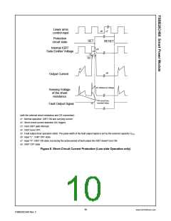
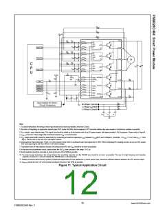
15V-Line
RE(H)
RBS
DBS
One-Leg Diagram of SPM
P
Vcc VB
IN
HO
0.1uF
22uF
COM VS
Inverter
Output
Vcc
IN
OUT
VSL
1000uF
1uF
COM
N
Note:
1. It would be recommended that the bootstrap diode, D , has soft and fast recovery characteristics.
BS
2. The bootstrap resistor (R ) should be 3 times greater than R
BS
. The recommended value of R
is 5.6Ω, but it can be increased up to 20Ω (maximum) for a slower dv/dt of
E(H)
E(H)
high-side.
3. The ceramic capacitor placed between V -COM should be over 1µF and mounted as close to the pins of the SPM as possible.
Figure 10.CCRecommended Bootstrap Operation Circuit and Parameters
11
www.fairchildsemi.com
FSBB20CH60 Rev. C

 FAIRCHILD [ FAIRCHILD SEMICONDUCTOR ]