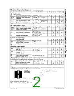
Electrical Characteristics TJ = 25°C unless otherwise noted
Symbol
Parameter
Test Conditions
Min
Typ
Max
Units
Off Characteristics
BVDSS
Drain to Source Breakdown Voltage ID = 250µA, VGS = 0V
40
V
∆BVDSS
∆TJ
Breakdown Voltage Temperature
Coefficient
ID = 250µA, referenced to 25°C
VDS = 32V, VGS = 0V
TJ = 55°C
VGS = ±20V,VDS = 0V
33
mV/°C
1
µA
µA
nA
IDSS
IGSS
Zero Gate Voltage Drain Current
Gate to Source Leakage Current
10
±100
On Characteristics (Note 2)
VGS(th)
Gate to Source Threshold Voltage VGS = VDS, ID = 250µA
1
1.9
3
V
∆VGS(th)
∆TJ
Gate to Source Threshold Voltage
ID = 250µA, referenced to 25°C
Temperature Coefficient
-4.6
mV/°C
VGS = 10V, ID = 6A
21
26
29
22
29
36
43
rDS(on)
gFS
Drain to Source On Resistance
Forward Transconductance
VGS = 4.5V, ID = 4.5A
VGS = 10V, ID = 6A,TJ = 125°C
VDS = 10V,ID = 6A
mΩ
S
Dynamic Characteristics
Ciss
Coss
Crss
Rg
Input Capacitance
715
105
60
955
140
90
pF
pF
pF
Ω
VDS = 20V, VGS = 0V,
f = 1MHz
Output Capacitance
Reverse Transfer Capacitance
Gate Resistance
f = 1MHz
1.1
Switching Characteristics
td(on)
tr
td(off)
tf
Turn-On Delay Time
Rise Time
9
5
18
10
37
6
ns
ns
VDD = 20V, ID = 1A
VGS = 10V, RGEN = 6Ω
Turn-Off Delay Time
Fall Time
23
3
ns
ns
Qg
Total Gate Charge
Gate to Source Gate Charge
Gate to Drain “Miller”Charge
7.7
2.4
2.8
11
nC
nC
nC
Qgs
Qgd
VDS = 20V, ID = 6A,VGS = 5V
Drain-Source Diode Characteristics and Maximum Ratings
VSD
trr
Source to Drain Diode Forward Voltage VGS = 0V, IS = 6A (note 2)
0.8
17
7
1.2
26
11
V
Reverse Recovery Time (note 3)
IF = 6A, diF/dt = 100A/µs
ns
nC
Qrr
Reverse Recovery Charge
Notes:
1: R
is the sum of the junction-to-case and case-to- ambient thermal resistance where the case thermal reference is defined as the solder mounting surface of the
θJA
drain pins. R
is guaranteed by design while R
is determined by the user’s board design.
θJA
θJC
a) 81°C/W when
mounted on a 1in
pad of 2 oz copper
b) 135°C/W when mounted on a
minimum pad .
2
Scale 1:1 on letter size paper
2: Pulse Test: Pulse Width < 300 us, Duty Cycle < 2.0%.
3: Starting T = 25°C, L = 1mH, I = 7.3A, V = 40V, V = 10V.
J
AS
DD
GS
FDS8949 Rev. B1
2
www.fairchildsemi.com

 FAIRCHILD [ FAIRCHILD SEMICONDUCTOR ]