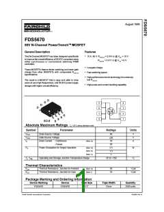
Typical Characteristics (continued)
10
5000
4000
3000
2000
1000
0
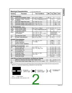
VDS = 10V
f = 1MHz
VGS = 0 V
ID = 10A
20V
8
30V
CISS
6
4
2
0
COSS
CRSS
0
10
20
30
40
50
0
10
20
30
Qg, GATE CHARGE (nC)
VDS, DRAIN TO SOURCE VOLTAGE (V)
Figure 7. Gate-Charge Characteristics.
Figure 8. Capacitance Characteristics.
100
50
40
30
20
10
0
RDS(ON) LIMIT
100µs
1ms
10ms
100ms
1s
10s
SINGLE PULSE
RθJA=125°C/W
10
1
TA = 25°C
DC
VGS = 10V
SINGLE PULSE
0.1
0.01
R
θJA = 125oC/W
TA = 25oC
0.1
1
10
100
0.001
0.01
0.1
1
10
100 300
VDS, DRAIN-SOURCE VOLTAGE (V)
SINGLE PULSE TIME (SEC)
Figure 9. Maximum Safe Operating Area.
Figure 10. Single Pulse Maximum
Power Dissipation.
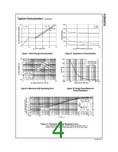
1
D = 0.5
0.5
R
(t) = r(t) * R
JA
θ
J A
θ
0.2
0.2
R
= 125°C/W
J A
θ
0. 1
0.1
00. 5
0.05
P(pk )
00. 2
t
0.02
1
0. 0 1
t
2
0.01
S i
n
g le P ul s e
T
- T = P
*
R
( )t
JA
J
A
θ
00. 05
Du t
y
C y c l e, D= t /t
2
1
00. 02
00. 01
0.0001
0.001
0.01
0.1
, TIME (se c)
1
10
100
300
t
1
Figure 11. Transient Thermal Response Curve.
Thermal characterization performed using the conditions described in Note 1c.
Transient themal response will change depending on the circuit board design.
FDS5670 Rev. B

 FAIRCHILD [ FAIRCHILD SEMICONDUCTOR ]