Electrical Characteristics
TA = 25°C unless otherwise noted
Symbol
Parameter
Test Conditions
Min Typ Max Units
Off Characteristics
BVDSS
Drain-Source Breakdown Voltage
60
V
VGS = 0 V, ID = 250 µA
Breakdown Voltage Temperature
Coefficient
58
∆BVDSS
∆TJ
ID = 250 µA, Referenced to 25°C
mV/°C
IDSS
Zero Gate Voltage Drain Current
VDS = 48 V, VGS = 0 V
1
µA
nA
nA
IGSSF
IGSSR
Gate-Body Leakage Current, Forward VGS = 20 V, VDS = 0 V
Gate-Body Leakage Current, Reverse VGS = -20 V, VDS = 0 V
100
-100
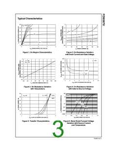
On Characteristics (Note 2)
VGS(th)
Gate Threshold Voltage
2
2.4
6.8
4
V
VDS = VGS, ID = 250 µA
Gate Threshold Voltage
Temperature Coefficient
∆VGS(th)
∆TJ
ID = 250 µA, Referenced to 25°C
mV/°C
RDS(on)
Static Drain-Source
On-Resistance
VGS = 10 V, ID = 10 A
VGS = 10 V, ID = 10 A, TJ=125°C
0.012 0.014
0.019 0.027
0.014 0.017
Ω
V
GS = 6 V, ID = 9 A
ID(on)
gFS
On-State Drain Current
VGS = 10 V, VDS = 5 V
25
A
S
Forward Transconductance
VDS = 5 V, ID = 10 A
39
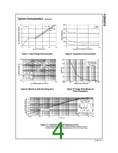
Dynamic Characteristics
Ciss
Coss
Crss
Input Capacitance
VDS = 15 V, VGS = 0 V
f = 1.0 MHz
2900
685
pF
pF
pF
Output Capacitance
Reverse Transfer Capacitance
180
Switching Characteristics (Note 2)
td(on)
tr
td(off)
tf
Turn-On Delay Time
Turn-On Rise Time
Turn-Off Delay Time
Turn-Off Fall Time
Total Gate Charge
Gate-Source Charge
Gate-Drain Charge
V
DD = 30 V, ID = 1 A
16
10
50
23
49
9
29
20
80
42
70
ns
ns
VGS = 10 V, RGEN = 6 Ω
ns
ns
Qg
VDS = 20 V, ID = 10 A
VGS = 10 V,
nC
nC
nC
Qgs
Qgd
10.4
Drain-Source Diode Characteristics and Maximum Ratings
IS
Maximum Continuous Drain-Source Diode Forward Current
2.1
1.2
A
V
VSD
Drain-Source Diode Forward Voltage VGS = 0 V, IS = 2.1 A (Note 2)
0.72
Notes:
1. RθJA is the sum of the junction-to-case and case-to-ambient thermal resistance where the case thermal reference is defined as the solder mounting surface of the
drain pins. RθJC is guaranteed by design while RθJA is determined by the user's board design.
c) 125° C/W when mounted
on a minimum pad.
a) 50° C/W when
b) 105° C/W when
mounted on a 0.5 in2
pad of 2 oz. copper.
mounted on a 0.02 in2
pad of 2 oz. copper.
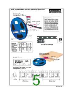
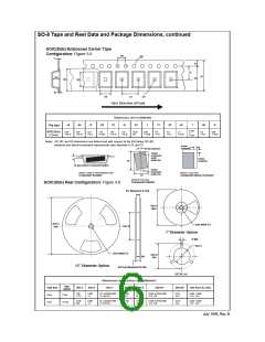
Scale
1 : 1 on letter size paper
2. Pulse Test: Pulse Width ≤ 300 µs, Duty Cycle ≤ 2.0%
FDS5670 Rev. B

 FAIRCHILD [ FAIRCHILD SEMICONDUCTOR ]