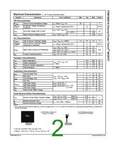
Electrical Characteristics TJ = 25°C unless otherwise noted
Symbol
Parameter
Test Conditions
Min
Typ
Max
Units
Off Characteristics
BVDSS
Drain to Source Breakdown Voltage
ID = 250µA, VGS = 0V
30
V
∆BVDSS
∆TJ
Breakdown Voltage Temperature
Coefficient
ID = 250µA, referenced to 25°C
22
mV/°C
VDS = 24V, VGS = 0V
TJ = 125°C
1
IDSS
IGSS
Zero Gate Voltage Drain Current
Gate to Source Leakage Current
µA
250
±100
VGS = ±20V, VDS = 0V
nA
On Characteristics
VGS(th)
Gate to Source Threshold Voltage
VGS = VDS, ID = 250µA
1.2
1.9
-6
2.5
V
∆VGS(th)
∆TJ
Gate to Source Threshold Voltage
Temperature Coefficient
ID = 250µA, referenced to 25°C
mV/°C
VGS = 10V, ID = 9.0A
16
22
22
24
19
30
30
rDS(on)
gFS
Static Drain to Source On Resistance
Forward Transconductance
VGS = 4.5V, ID = 7.2A
mΩ
VGS = 10V, ID = 9.0A, TJ = 125°C
VDD = 5V, ID = 9.0A
S
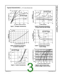
Dynamic Characteristics
Ciss
Coss
Crss
Rg
Input Capacitance
513
110
76
685
150
115
2.1
pF
pF
pF
Ω
VDS = 15V, VGS = 0V,
f = 1MHz
Output Capacitance
Reverse Transfer Capacitance
Gate Resistance
f = 1MHz
1.4
Switching Characteristics
td(on)
tr
td(off)
tf
Turn-On Delay Time
Rise Time
6
2
12
10
27
10
14
7.0
ns
ns
VDD = 15V, ID = 9.0A,
VGS = 10V, RGEN = 6Ω
Turn-Off Delay Time
Fall Time
15
2
ns
ns
Total Gate Charge
Total Gate Charge
Total Gate Charge
Gate to Drain “Miller” Charge
VGS = 0V to 10V
10
5.0
1.8
2.2
nC
nC
nC
nC
Qg(TOT)
VGS = 0V to 4.5V
VDD = 15V
ID = 9.0A
Qgs
Qgd
Drain-Source Diode Characteristics
VGS = 0V, IS = 9.0A
VGS = 0V, IS = 1.6A
(Note 2)
(Note 2)
0.86
0.76
13
1.2
1.2
18
VSD
Source to Drain Diode Forward Voltage
V
trr
Reverse Recovery Time
ns
IF = 9.0A, di/dt = 100A/µs
Qrr
Reverse Recovery Charge
3
10
nC
NOTES:
2
1. R
is determined with the device mounted on a 1in pad 2 oz copper pad on a 1.5 x 1.5 in. board of FR-4 material. R
is guaranteed by design while R
is determined by
θJA
θJC
θCA
the user's board design.
a.
125°C/W when mounted on a
minimum pad of 2 oz copper
b.
53°C/W when mounted on a
1 in pad of 2 oz copper
2
2. Pulse Test: Pulse Width < 300µs, Duty cycle < 2.0%.
o
3. Starting T = 25 C; N-ch: L = 1mH, I = 7A, V = 30V, V = 10V.
J
AS
DD
GS
www.fairchildsemi.com
FDMC8884 Rev.C
2

 FAIRCHILD [ FAIRCHILD SEMICONDUCTOR ]