Package Marking and Ordering Information
Device Marking
Device
Package
Reel Size
Tape Width
Quantity
FDA69N25
FDA69N25
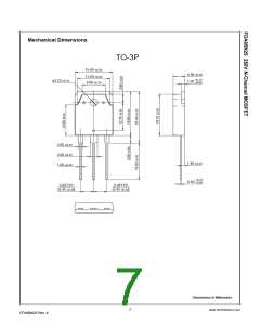
TO-3P
--
--
30
Electrical Characteristics
T
= 25°C unless otherwise noted
C
Symbol
Parameter
Test Conditions
Min
Typ Max Units
Off Characteristics
BVDSS
Drain-Source Breakdown Voltage
VGS = 0 V, ID = 250 µA
250
--
--
--
V
∆BVDSS
∆TJ
/
Breakdown Voltage Temperature Coefficient ID = 250 µA, Referenced to 25°C
--
0.25
V/°C
IDSS
Zero Gate Voltage Drain Current
VDS = 250 V, VGS = 0 V
VDS = 200 V, TC = 125°C
VGS = 30 V, VDS = 0 V
VGS = -30 V, VDS = 0 V
--
--
--
--
--
--
--
--
1
µA
µA
nA
nA
10
IGSSF
IGSSR
Gate-Body Leakage Current, Forward
Gate-Body Leakage Current, Reverse
100
-100
On Characteristics
VGS(th)
RDS(on)
gFS
Gate Threshold Voltage
VDS = VGS, ID = 250 µA
VGS = 10 V, ID = 34.5 A
VDS = 40 V, ID = 34.5 A
3.0
--
--
0.034
25
5.0
0.041
--
V
Ω
S
Static Drain-Source On-Resistance
Forward Transconductance
(Note 4)
--
Dynamic Characteristics
Ciss
Coss
Crss
Input Capacitance
VDS = 25 V, VGS = 0 V,
f = 1.0 MHz
--
--
--
3570
750
84
4640
980
pF
pF
pF
Output Capacitance
Reverse Transfer Capacitance
130
Switching Characteristics
td(on) Turn-On Delay Time
tr
td(off)
tf
VDD = 125 V, ID = 69A,
--
--
--
--
--
--
--
ns
ns
95
855
130
220
77
200
1720
270
RG = 25 Ω
Turn-On Rise Time
Turn-Off Delay Time
Turn-Off Fall Time
Total Gate Charge
Gate-Source Charge
Gate-Drain Charge
ns
(Note 4, 5)
ns
450
Qg
VDS = 200 V, ID = 69A,
GS = 10 V
nC
nC
nC
100
--
V
Qgs
Qgd
24
(Note 4, 5)
--
37
Drain-Source Diode Characteristics and Maximum Ratings
IS
Maximum Continuous Drain-Source Diode Forward Current
Maximum Pulsed Drain-Source Diode Forward Current
--
--
--
--
--
--
--
34
136
1.4
--
A
A
ISM
VSD
trr
Drain-Source Diode Forward Voltage
Reverse Recovery Time
VGS = 0 V, IS = 69 A
--
V
VGS = 0 V, IS = 69 A,
210
5.7
ns
dIF / dt = 100 A/µs
(Note 4)
Qrr
Reverse Recovery Charge
--
µC
NOTES:
1. Repetitive Rating : Pulse width limited by maximum junction temperature
2. L = 0.64mH, I =69A, V = 50V, R = 25 Ω, Starting T = 25°C
AS
DD
G
J
3. I ≤ 69A, di/dt ≤200A/µs, V ≤ BV
Starting T = 25°C
J
SD
DD
DSS,
4. Pulse Test : Pulse width ≤ 300µs, Duty cycle ≤ 2%
5. Essentially independent of operating temperature
2
www.fairchildsemi.com
FDA69N25 Rev. A

 FAIRCHILD [ FAIRCHILD SEMICONDUCTOR ]