Package Marking and Ordering Information TC = 25oC unless otherwise noted
Device Marking
Device
Package
Reel Size
Tape Width
Quantity
FCD9N60N
FCD9N60NTM
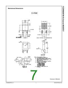
D-PAK
380mm
16mm
2500
Electrical Characteristics
Symbol
Parameter
Test Conditions
Min.
Typ.
Max.
Units
Off Characteristics
BVDSS
Drain to Source Breakdown Voltage
ID = 1mA, VGS = 0V, TJ = 25oC
600
-
-
-
V
ΔBVDSS
ΔTJ
Breakdown Voltage Temperature
Coefficient
I
D = 1mA, Referenced to 25oC
-
-
0.8
V/oC
V
DS = 480V, VGS = 0V
-
-
-
10
IDSS
IGSS
Zero Gate Voltage Drain Current
Gate to Body Leakage Current
μA
VDS = 480V, VGS = 0V, TC = 125oC
-
-
100
VGS = ±30V, VDS = 0V
±100
nA
On Characteristics
VGS(th)
RDS(on)
gFS
Gate Threshold Voltage
VGS = VDS, ID = 250μA
VGS = 10V, ID = 4.5A
VDS = 40V, ID = 4.5A
3.0
-
5.0
0.385
-
V
Ω
S
Static Drain to Source On Resistance
Forward Transconductance
-
-
0.330
5.3
Dynamic Characteristics
Ciss
Input Capacitance
-
-
-
-
-
735
40
1000
pF
pF
pF
pF
pF
VDS = 100V, VGS = 0V
f = 1MHz
Coss
Crss
Output Capacitance
53
5.5
-
Reverse Transfer Capacitance
Output Capacitance
3.5
Coss
Cosseff.
VDS = 380V, VGS = 0V, f = 1MHz
VDS = 0V to 380V, VGS = 0V
23.7
122
Effective Output Capacitance
-
Switching Characteristics
td(on)
tr
td(off)
tf
Turn-On Delay Time
Turn-On Rise Time
-
-
-
-
-
-
13.2
9.6
-
-
-
-
-
-
ns
ns
ns
ns
nC
nC
VDD = 380V, ID = 4.5A
R
GEN = 4.7Ω
Turn-Off Delay Time
Turn-Off Fall Time
28.7
11.5
17.8
4.2
(Note 4)
(Note 4)
Qg(tot)
Qgs
Total Gate Charge at 10V
Gate to Source Gate Charge
V
DS = 380V, ID = 4.5A
VGS = 10V
Qgd
Gate to Drain “Miller” Charge
-
-
7.6
-
-
nC
ESR
Equivalent Series Resistance(G-S)
Drain Open
2.65
Ω
Drain-Source Diode Characteristics
IS
Maximum Continuous Drain to Source Diode Forward Current
Maximum Pulsed Drain to Source Diode Forward Current
-
-
-
-
-
9.0
27
-
A
A
ISM
VSD
trr
-
1.2
-
Drain to Source Diode Forward Voltage
Reverse Recovery Time
VGS = 0V, ISD = 9A
-
V
322
5.04
ns
μC
VGS = 0V, ISD = 9A
dIF/dt = 100A/μs
Qrr
Reverse Recovery Charge
-
Notes:
1. Repetitive Rating: Pulse width limited by maximum junction temperature
2. I = 3A, R = 25Ω, Starting T = 25°C
AS
G
J
3. I ≤ 9A, di/dt ≤ 200A/μs, V ≤ 380V, Starting T = 25°C
SD
DD
J
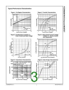
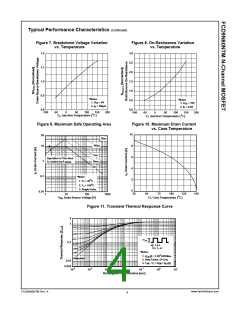
4. Essentially Independent of Operating Temperature Typical Characteristics
www.fairchildsemi.com
FCD9N60NTM Rev. A
2

 FAIRCHILD [ FAIRCHILD SEMICONDUCTOR ]