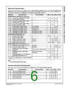
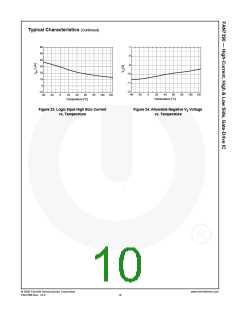
Electrical Characteristics
VBIAS (VDD, VBS)=15.0V, VS=VSS=COM, TA=25°C, unless otherwise specified. The VIL, VIH, and IIN parameters are
referenced to VSS/COM and are applicable to the respective input signals HIN and LIN. The VO and IO parameters are
referenced to COM and VS is applicable to the respective output signals HO and LO.
Symbol
Characteristics
Test Condition
Min. Typ. Max. Unit
POWER SUPPLY SECTION (VDD AND VBS
)
VDDUV+ VDD and VBS Supply Under-Voltage
VBSUV+ Positive-going Threshold
8.0
7.4
8.8
8.3
0.5
9.8
9.0
VDDUV- VDD and VBS Supply Under-Voltage
VBSUV- Negative-going Threshold
V
VDDUVH VDD and VBS Supply Under-Voltage
VBSUVH Lockout Hysteresis Voltage
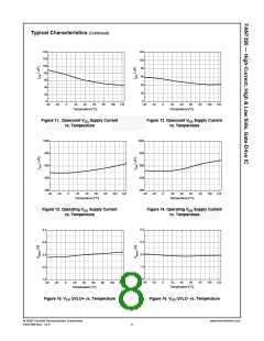
ILK
Offset Supply Leakage Current
Quiescent VBS Supply Current
Quiescent VDD Supply Current
Operating VBS Supply Current
Operating VDD Supply Current
VB=VS=600V
50
80
IQBS
IQDD
IPBS
IPDD
VIN=0V or 5V
45
75
µA
µA
VIN=0V or 5V
110
640
640
fIN=20kHz, rms value
fIN=20kHz, rms value
530
530
LOGIC INPUT SECTION (HIN, LIN)
VIH
VIL
IIN+
IIN-
RIN
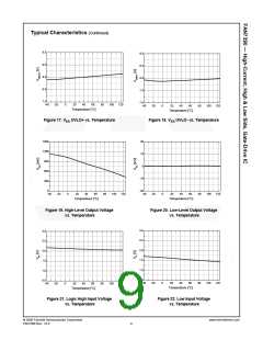
Logic "1" Input Voltage
2.5
V
Logic "0" Input Voltage
1.2
50
Logic "1" Input Bias Current
Logic "0" Input Bias Current
Input Pull-down Resistance
VIN=5V
VIN=0V
25
1.0
200
µA
2.0
100
KΩ
GATE DRIVER OUTPUT SECTION (HO, LO)
VOH
VOL
High-level Output Voltage, VBIAS-VO
Low-level Output Voltage, VO
No Load
No Load
1.0
35
V
mV
Output High, Short-circuit Pulsed
Current(4)
IO+
IO-
VS
VO=0V, VIN=5V with PW<10µs
3.5
3.5
4.5
4.5
A
Output Low, Short-circuit Pulsed
Current(4)
VO=15V, VIN=0V with
PW<10µs
Allowable Negative VS Pin Voltage for
HIN Signal Propagation to HO
-9.8
-7.0
7.0
V
V
VSS
COM
-
VSS-COM/COM-VSS Voltage Educability
-7.0
Note:
4. This parameter guaranteed by design.
Dynamic Electrical Characteristics
VBIAS (VDD, VBS)=15.0V, VS=VSS=COM=0V, CL=1000pF and TA=25°C unless otherwise specified.
Symbol
Characteristics
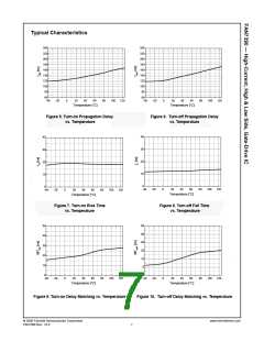
Turn-on Propagation Delay
Turn-off Propagation Delay
Delay Matching, HS & LS Turn-on/off
Turn-on Rise Time
Test Condition
VS=0V
Min. Typ. Max. Unit
ton
toff
MT
tr
140
140
0
200
200
50
VS=0V
ns
25
20
50
tf
Turn-off Fall Time
45
© 2008 Fairchild Semiconductor Corporation
FAN7390 Rev. 1.0.2
www.fairchildsemi.com
6

 FAIRCHILD [ FAIRCHILD SEMICONDUCTOR ]