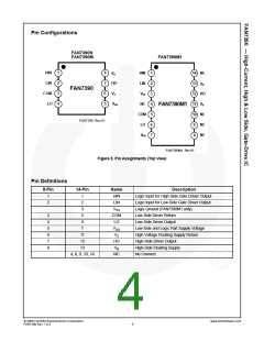
Pin Configurations
FAN7390N
FAN7390M
FAN7390M1
HIN
LIN
1
2
3
4
8
7
6
5
HIN
LIN
VSS
1
2
3
4
5
6
7
14 NC
VB
HO
VS
13
12
11
10
9
VB
FAN7390
COM
LO
HO
VS
VDD
NC
FAN7390M1
COM
LO
NC
NC
NC
FAN7390 Rev.01
VDD
8
FAN7390M1 Rev.01
Figure 5. Pin Assignments (Top View)
Pin Definitions
8-Pin
14-Pin
Name
Description
1
2
1
HIN
LIN
VSS
COM
LO
Logic Input for High-Side Gate Driver Output
Logic Input for Low-Side Gate Driver Output
Logic Ground (FAN7390M1 only)
Low-Side Driver Return
2
3
3
4
5
6
7
8
5
6
Low-Side Driver Output
7
VDD
VS
Low-Side and Logic Part Supply Voltage
High-Voltage Floating Supply Return
High-Side Driver Output
11
12
13
HO
VB
High-Side Floating Supply
4, 8, 9, 10, 14
NC
No Connect
© 2008 Fairchild Semiconductor Corporation
FAN7390 Rev. 1.0.2
www.fairchildsemi.com
4

 FAIRCHILD [ FAIRCHILD SEMICONDUCTOR ]