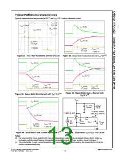
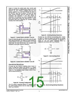
Figure 47 shows the pulsed gate drive current path
when the gate driver is supplying gate charge to turn the
MOSFET on. The current is supplied from the local
bypass capacitor CBYP and flows through the driver to
the MOSFET gate and to ground. To reach the high
peak currents possible with the FAN312x family, the
resistance and inductance in the path should be
minimized. The localized CBYP acts to contain the high
peak current pulses within this driver-MOSFET circuit,
preventing them from disturbing the sensitive analog
circuitry in the PWM controller.
VDD
Turn-on threshold
IN-
IN+
VDD
VDS
(VDD
)
CBYP
FAN3121/2
OUT
PWM
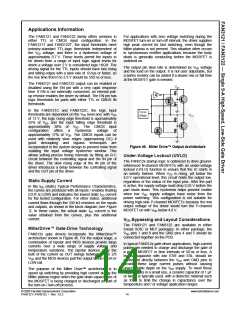
Figure 50. Inverting Startup Waveforms
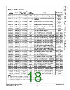
At power up, the FAN3122 non-inverting driver, shown
in Figure 51, holds the output LOW until the VDD voltage
reaches the UVLO turn-on threshold, as indicated in
Figure 52. The OUT pulses magnitude follow VDD
magnitude until steady-state VDD is reached.
Figure 47. Current Path for MOSFET Turn-On
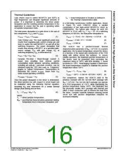
Figure 48 shows the path the current takes when the gate
driver turns the MOSFET off. Ideally, the driver shunts the
current directly to the source of the MOSFET in a small
circuit loop. For fast turn-off times, the resistance and
inductance in this path should be minimized.
V
DD
VDD
VDS
IN
OUT
CBYP
FAN3121/2
Figure 51. Non-Inverting Driver
PWM
VDD
Turn-on threshold
Figure 48. Current Path for MOSFET Turn-Off
Operational Waveforms
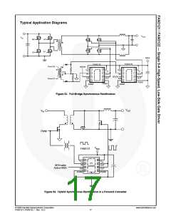
At power up, the FAN3121 inverting driver shown in
Figure 49 holds the output LOW until the VDD voltage
reaches the UVLO turn-on threshold, as indicated in
Figure 50. This facilitates proper startup control of low-
side N-channel MOSFETs.
IN-
IN+
VDD
IN
OUT
OUT
Figure 49. Inverting Configuration
The OUT pulses’ magnitude follows VDD magnitude with
the output polarity inverted from the input until steady-
state VDD is reached.
Figure 52. Non-Inverting Startup Waveforms
© 2008 Fairchild Semiconductor Corporation
FAN3121 / FAN3122 • Rev. 1.0.2
www.fairchildsemi.com
15

 FAIRCHILD [ FAIRCHILD SEMICONDUCTOR ]