Applications Information
The FAN3121 and FAN3122 family offers versions in
either TTL or CMOS input configuration. In the
FAN3121T and FAN3122T, the input thresholds meet
industry-standard TTL-logic thresholds independent of
the VDD voltage, and there is a hysteresis voltage of
approximately 0.7 V. These levels permit the inputs to
be driven from a range of input logic signal levels for
which a voltage over 2 V is considered logic HIGH. The
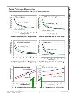
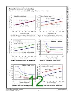
driving signal for the TTL inputs should have fast rising
and falling edges with a slew rate of 6V/µs or faster, so
the rise time from 0 to 3.3 V should be 550 ns or less.
For applications with zero voltage switching during the
MOSFET turn-on or turn-off interval, the driver supplies
high peak current for fast switching, even though the
Miller plateau is not present. This situation often occurs
in synchronous rectifier applications because the body
diode is generally conducting before the MOSFET is
switched on.
The output pin slew rate is determined by VDD voltage
and the load on the output. It is not user adjustable, but
a series resistor can be added if a slower rise or fall time
at the MOSFET gate is needed.
The FAN3121 and FAN3122 output can be enabled or
disabled using the EN pin with a very rapid response
time. If EN is not externally connected, an internal pull-
up resistor enables the driver by default. The EN pin has
logic thresholds for parts with either TTL or CMOS IN
thresholds.
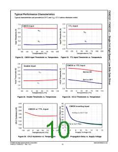
In the FAN3121C and FAN3122C, the logic input
thresholds are dependent on the VDD level and, with VDD
of 12 V, the logic rising edge threshold is approximately
55% of VDD and the input falling edge threshold is
approximately 38% of VDD
.
The CMOS input
voltage of
configuration offers hysteresis
a
approximately 17% of VDD. The CMOS inputs can be
used with relatively slow edges (approaching DC) if
good decoupling and bypass techniques are
incorporated in the system design to prevent noise from
violating the input voltage hysteresis window. This
allows setting precise timing intervals by fitting an R-C
circuit between the controlling signal and the IN pin of
the driver. The slow rising edge at the IN pin of the
driver introduces a delay between the controlling signal
and the OUT pin of the driver.
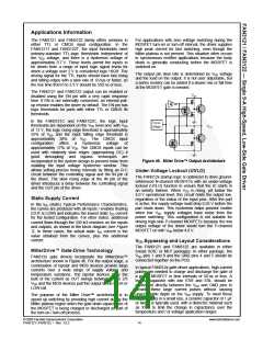
Figure 46. Miller Drive™ Output Architecture
Under-Voltage Lockout (UVLO)
The FAN312x startup logic is optimized to drive ground-
referenced N-channel MOSFETs with an under-voltage
lockout (UVLO) function to ensure that the IC starts in
an orderly fashion. When VDD is rising, yet below the
4.0 V operational level, this circuit holds the output low,
regardless of the status of the input pins. After the part
is active, the supply voltage must drop 0.25 V before the
part shuts down. This hysteresis helps prevent chatter
when low VDD supply voltages have noise from the
power switching. This configuration is not suitable for
driving high-side P-channel MOSFETs because the low
output voltage of the driver would turn the P-channel
MOSFET on with VDD below 4.0 V.
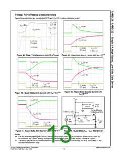
Static Supply Current
In the IDD (static) Typical Performance Characteristics,
the curves are produced with all inputs / enables floating
(OUT is LOW) and indicates the lowest static IDD current
for the tested configuration. For other states, additional
current flows through the 100 k resistors on the inputs
and outputs, as shown in the block diagram (see Figure
7). In these cases, the actual static IDD current is the
value obtained from the curves, plus this additional
current.
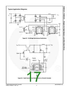
VDD Bypassing and Layout Considerations
The FAN3121 and FAN3122 are available in either
8-lead SOIC or MLP packages. In either package, the
VDD pins 1 and 8 and the GND pins 4 and 5 should be
connected together on the PCB.
MillerDrive™ Gate-Drive Technology
FAN312x gate drivers incorporate the MillerDrive™
architecture shown in Figure 46. For the output stage, a
combination of bipolar and MOS devices provide large
currents over a wide range of supply voltage and
temperature variations. The bipolar devices carry the
bulk of the current as OUT swings between 1/3 to 2/3
In typical FAN312x gate-driver applications, high-current
pulses are needed to charge and discharge the gate of
a power MOSFET in time intervals of 50 ns or less. A
bypass capacitor with low ESR and ESL should be
connected directly between the VDD and GND pins to
provide these large current pulses without causing
unacceptable ripple on the VDD supply. To meet these
requirements in a small size, a ceramic capacitor of 1 µF
or larger is typically used, with a dielectric material such
as X7R, to limit the change in capacitance over the
temperature and / or voltage application ranges.
VDD and the MOS devices pull the output to the HIGH or
LOW rail.
The purpose of the Miller Drive™ architecture is to
speed up switching by providing high current during the
Miller plateau region when the gate-drain capacitance of
the MOSFET is being charged or discharged as part of
the turn-on / turn-off process.
© 2008 Fairchild Semiconductor Corporation
FAN3121 / FAN3122 • Rev. 1.0.2
www.fairchildsemi.com
14

 FAIRCHILD [ FAIRCHILD SEMICONDUCTOR ]