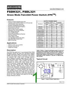
FSDH321, FSDL321
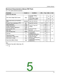
Electrical Characteristics (Sense FET Part)
(Ta = 25°C unless otherwise specified)
Parameter
Symbol
Condition
Min.
Typ. Max.
Unit
Sense FET SECTION
V
V
=Max. Rating,
=0V
DS
GS
-
-
-
-
-
25
200
19
µA
µA
Zero Gate Voltage Drain Current
I
DSS
V
=0.8Max. Rating,
DS
GS
V
=0V, T =125°C
C
Static Drain-Source on Resistance
R
V
GS
V
DS
=10V, I =0.5A
D
14
Ω
DS(ON)
gfs
(Note)
Forward Trans conductance (Note)
Input Capacitance
Output Capacitance
Reverse Transfer Capacitance
Turn on Delay Time
=50V, I =0.5A
D
1.0
1.3
162
18
3.8
9.5
19
-
-
-
-
-
-
-
S
C
-
-
-
-
-
-
ISS
V
=0V, V =25V,
DS
GS
C
C
pF
ns
OSS
RSS
f=1MHz
td(on)
tr
td(off)
V
=0.5B V ,
DSS
DD
I =1.0A
D
Rise Time
Turn Off Delay Time
(MOSFET switching time
is essentially
33
independent of
Fall Time
tf
-
42
-
operating temperature)
Total Gate Charge
V
=10V, I =1.0A,
D
GS
DS
Qg
-
-
7.0
3.1
-
-
(Gate-Source + Gate-Drain)
V
=0.5B V
DSS
(MOSFET switching time
is essentially
Gate-Source Charge
Qgs
nC
independent of operating
temperature)
Gate-Drain (Miller) Charge
Qgd
-
0.4
-
Note:
1. Pulse test: Pulse width ≤ 300µS, duty ≤ 2%
2.
1
S = ---
R
5

 FAIRCHILD [ FAIRCHILD SEMICONDUCTOR ]