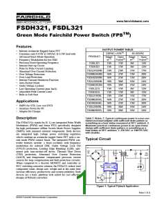
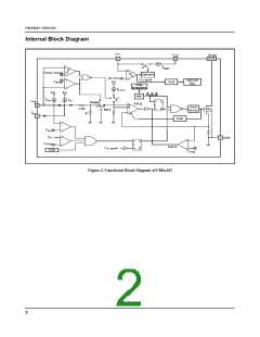
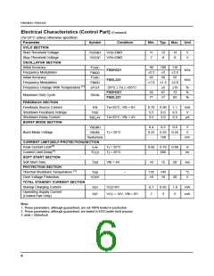
FSDH321, FSDL321
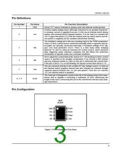
Pin Definitions
Pin Number
Pin Name
Pin Function Description
1
GND
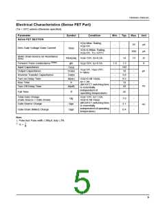
Sense FET source terminal on primary side and internal control ground.
Positive supply voltage input. Although connected to an auxiliary transform-
er winding, current is supplied from pin 5 (Vstr) via an internal switch during
startup (see Internal Block Diagram section). It is not until Vcc reaches the
UVLO upper threshold (12V) that the internal start-up switch opens and de-
vice power is supplied via the auxiliary transformer winding.
The feedback voltage pin is the non-inverting input to the PWM comparator.
It has a 0.9mA current source connected internally while a capacitor and op-
tocoupler are typically connected externally. A feedback voltage of 6V trig-
gers over load protection (OLP). There is a time delay while charging
between 3V and 6V using an internal 5uA current source, which prevents
false triggering under transient conditions but still allows the protection
mechanism to operate under true overload conditions.
2
3
Vcc
Vfb
Pin to adjust the current limit of the Sense FET. The feedback 0.9mA current
source is diverted to the parallel combination of an internal 2.8kΩ resistor
and any external resistor to GND on this pin to determine the current limit.
If this pin is tied to Vcc or left floating, the typical current limit will be 0.7A.
This pin connects directly to the rectified AC line voltage source. At start up
the internal switch supplies internal bias and charges an external storage
capacitor placed between the Vcc pin and ground. Once the Vcc reaches
12V, the internal switch is disabled.
4
5
Ipk
Vstr
The Drain pin is designed to connect directly to the primary lead of the trans-
former and is capable of switching a maximum of 650V. Minimizing the
length of the trace connecting this pin to the transformer will decrease leak-
age inductance.
6, 7, 8
Drain
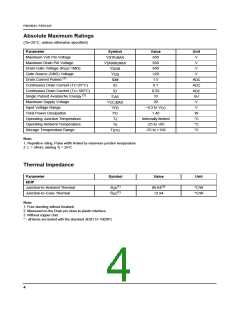
Pin Configuration
8DIP
8LSOP
Drain
Drain
GND 1
Vcc 2
8
7
Vfb
Ipk
6 Drain
3
4
5
Vstr
Figure 3. Pin Configuration (Top View)
3

 FAIRCHILD [ FAIRCHILD SEMICONDUCTOR ]