PDF
最近搜索
热门搜索
发布采购

| 型号: | CD4538 |
| PDF下载: | 下载PDF文件 查看货源 |
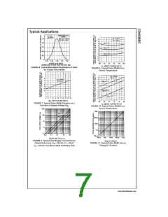
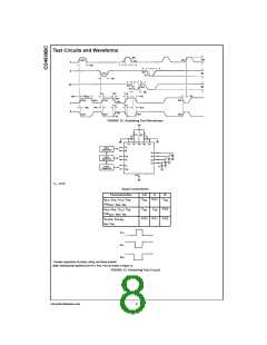
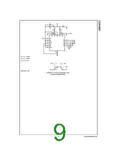
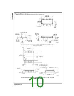
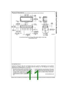
| 内容描述: | 双单稳态精度 [Dual Precision Monostable] |
| 分类和应用: | |
| 文件页数/大小: | 11 页 / 137 K |
| 品牌: |  FAIRCHILD [ FAIRCHILD SEMICONDUCTOR ] FAIRCHILD [ FAIRCHILD SEMICONDUCTOR ] |
专业IC领域供求交易平台:提供全面的IC Datasheet资料和资讯,Datasheet 1000万数据,IC品牌1000多家。