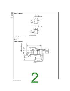
Theory of Operation
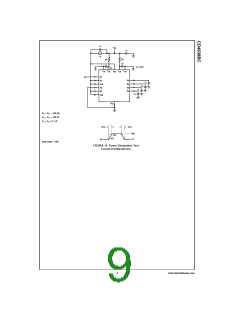
FIGURE 2.
Thus, propagation delay from trigger to Q is independent of
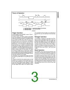
Trigger Operation
the value of CX, RX, or the duty cycle of the input wave-
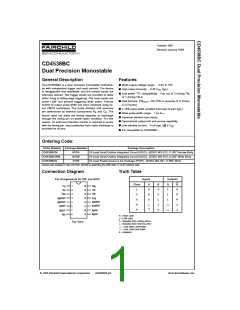
The block diagram of the CD4538BC is shown in Figure 1,
form.
with circuit operation following.
As shown in Figure 1 and Figure 2, before an input trigger
occurs, the monostable is in the quiescent state with the Q
output low, and the timing capacitor CX completely charged
Retrigger Operation
The CD4538BC is retriggered if a valid trigger occurs(3) fol-
lowed by another valid trigger(4) before the Q output has
returned to the quiescent (zero) state. Any retrigger, after
the timing node voltage at pin 2 or 14 has begun to rise
from VREF1, but has not yet reached VREF2, will cause an
to VDD. When the trigger input A goes from VSS to VDD
(while inputs B and CD are held to VDD) a valid trigger is
recognized, which turns on comparator C1 and N-Channel
transistor N1(1). At the same time the output latch is set.
increase in output pulse width T. When a valid retrigger is
initiated(4), the voltage at T2 will again drop to VREF1 before
progressing along the RC charging curve toward VDD. The
With transistor N1 on, the capacitor CX rapidly discharges
toward VSS until VREF1 is reached. At this point the output
of comparator C1 changes state and transistor N1 turns off.
Comparator C1 then turns off while at the same time com-
parator C2 turns on. With transistor N1 off, the capacitor CX
Q output will remain high until time T, after the last valid
retrigger.
begins to charge through the timing resistor, RX, toward
VDD. When the voltage across CX equals VREF2, compara-
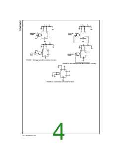
Reset Operation
The CD4538BC may be reset during the generation of the
output pulse. In the reset mode of operation, an input pulse
on CD sets the reset latch and causes the capacitor to be
tor C2 changes state causing the output latch to reset (Q
goes low) while at the same time disabling comparator C2.
This ends the timing cycle with the monostable in the qui-
escent state, waiting for the next trigger.
fast charged to VDD by turning on transistor Q1(5). When
A valid trigger is also recognized when trigger input B goes
the voltage on the capacitor reaches VREF2, the reset latch
from VDD to VSS (while input A is at VSS and input CD is at
(2)
will clear and then be ready to accept another pulse. If the
CD input is held low, any trigger inputs that occur will be
VDD
) .
It should be noted that in the quiescent state CX is fully
charged to VDD, causing the current through resistor RX to
inhibited and the Q and Q outputs of the output latch will
not change. Since the Q output is reset when an input low
level is detected on the CD input, the output pulse T can be
be zero. Both comparators are “off” with the total device
current due only to reverse junction leakages. An added
feature of the CD4538BC is that the output latch is set via
the input trigger without regard to the capacitor voltage.
made significantly shorter than the minimum pulse width
specification.
3
www.fairchildsemi.com

 FAIRCHILD [ FAIRCHILD SEMICONDUCTOR ]