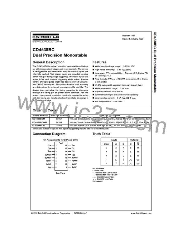
Absolute Maximum Ratings(Note 1)
(Note 2)
Recommended Operating
Conditions (Note 2)
DC Supply Voltage (VDD
)
−0.5 to +18 VDC
−0.5V to VDD + 0.5 VDC
−65°C to +150°C
DC Supply Voltage (VDD
Input Voltage (VIN
Operating Temperature Range (TA)
)
3 to 15 VDC
0 to VDD VDC
Input Voltage (VIN
)
)
Storage Temperature Range (TS)
Power Dissipation (PD)
Dual-In-Line
−40°C to +85°C
Note 1: “Absolute Maximum Ratings” are those values beyond which the
safety of the device cannot be guaranteed, they are not meant to imply that
the devices should be operated at these limits. The tables of “Recom-
mended Operating Conditions” and “Electrical Characteristics” provide con-
ditions for actual device operation.
700 mW
500 mW
Small Outline
Lead Temperature (TL)
(Soldering, 10 seconds)
Note 2: V = 0V unless otherwise specified.
SS
260°C
DC Electrical Characteristics (Note 2)
−40°C
+25°C
Typ
0.005
0.010
0.015
0
+85°C
Symbol
Parameter
Conditions
Units
Min
Max
Min
Max
20
Min
Max
I
Quiescent
V
V
V
V
V
V
V
V
V
= 5V
V
= V
20
40
150
300
600
0.05
0.05
0.05
µA
µA
µA
V
DD
DD
DD
DD
DD
DD
DD
DD
DD
DD
IH
DD
Device Current
= 10V
V
= V
40
IL
SS
= 15V All Outputs Open
80
80
V
V
V
LOW Level
= 5V
|I | < 1 µA
0.05
0.05
0.05
0.05
0.05
0.05
OL
OH
IL
O
Output Voltage
= 10V
= 15V
= 5V
V
= V , V = V
0
V
IH
DD
IL
SS
SS
0
V
HIGH Level
|I | < 1 µA
4.95
9.95
4.95
9.95
5
4.95
9.95
V
O
Output Voltage
= 10V
= 15V
V
= V , V = V
10
V
IH
DD
IL
14.95
14.95
15
14.95
V
LOW Level
|I | < 1 µA
O
Input Voltage
V
V
V
= 5V, V = 0.5V or 4.5V
1.5
3.0
4.0
2.25
4.50
6.75
1.5
3.0
4.0
1.5
3.0
4.0
V
V
V
DD
DD
DD
O
= 10V, V = 1.0V or 9.0V
O
= 15V, V = 1.5V or 13.5V
O
V
HIGH Level
|I | < 1 µA
O
IH
Input Voltage
V
V
V
V
V
V
V
V
V
V
= 5V, V = 0.5V or 4.5V
3.5
7.0
3.5
7.0
2.75
5.50
8.25
0.88
2.25
8.8
3.5
7.0
V
DD
DD
DD
DD
DD
O
= 10V, V = 1.0V or 9.0V
V
O
= 15V, V = 1.5V or 13.5V
11.0
0.52
1.3
11.0
0.44
1.1
11.0
0.36
0.9
V
O
I
I
LOW Level
Output Current
(Note 3)
= 5V, V = 0.4V
V
V
= V
mA
mA
mA
mA
mA
mA
µA
OL
O
IH
IL
DD
= 10V, V = 0.5V
= V
O
SS
= 15V, V = 1.5V
3.6
3.0
2.4
D
O
HIGH Level
Output Current
(Note 3)
= 5V, V = 4.6V
−0.52
−1.3
−3.6
−0.44 −0.88
−1.1 −2.25
−0.36
−0.9
−2.4
OH
IN
DD
DD
O
= 10V, V = 9.5V
V
= V
O
IL
SS
= 15V, V = 13.5V
−3.0
−8.8
D
O
−5
I
I
Input Current,
Pin 2 or 14
Input Current
Other Inputs
= 15V, V = 0V or 15V
±0.02
±0.3
±10
±0.05
±0.3
±0.5
±1.0
DD
IN
−5
V
= 15V, V = 0V or 15V
±10
µA
IN
DD
IN
Note 3: I
and I are tested one output at a time.
OL
OH
5
www.fairchildsemi.com

 FAIRCHILD [ FAIRCHILD SEMICONDUCTOR ]