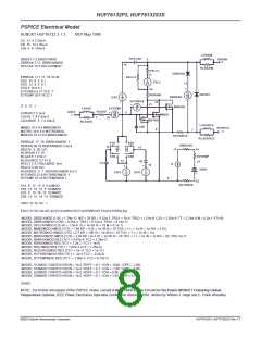
HUF76132P3, HUF76132S3S
o
Absolute Maximum Ratings
T = 25 C, Unless Otherwise Specified
C
UNITS
Drain to Source Voltage (Note 1). . . . . . . . . . . . . . . . . . . . . . . . . . . . . . . . . . . . . . . . . V
30
30
V
V
V
DSS
Drain to Gate Voltage (R
= 20kΩ) (Note 1) . . . . . . . . . . . . . . . . . . . . . . . . . . . . . . .V
GS
DGR
Gate to Source Voltage . . . . . . . . . . . . . . . . . . . . . . . . . . . . . . . . . . . . . . . . . . . . . . . . . V
±20
GS
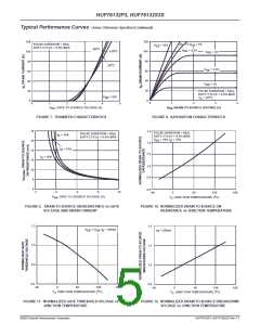
Drain Current
o
Continuous (T = 25 C, V
C
= 10V) (Figure 2) . . . . . . . . . . . . . . . . . . . . . . . . . . . . . .I
75
44
41
A
A
A
GS
D
D
o
Continuous (T = 100 C, V
= 5V) . . . . . . . . . . . . . . . . . . . . . . . . . . . . . . . . . . . . . . .I
= 4.5V) (Figure 2) . . . . . . . . . . . . . . . . . . . . . . . . . . . . .I
C
GS
o
Continuous (T = 100 C, V
C
GS
D
Pulsed Drain Current . . . . . . . . . . . . . . . . . . . . . . . . . . . . . . . . . . . . . . . . . . . . . . . . . I
Figure 4
DM
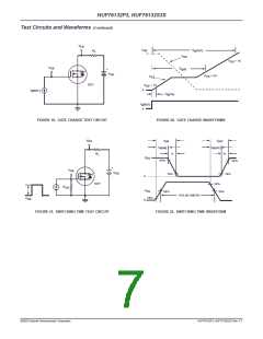
Pulsed Avalanche Rating. . . . . . . . . . . . . . . . . . . . . . . . . . . . . . . . . . . . . . . . . . . . . . . . E
Figures 6, 17, 18
AS
Power Dissipation . . . . . . . . . . . . . . . . . . . . . . . . . . . . . . . . . . . . . . . . . . . . . . . . . . . . . . P
Derate Above 25 C . . . . . . . . . . . . . . . . . . . . . . . . . . . . . . . . . . . . . . . . . . . . . . . . . . . . .
120
0.97
W
W/ C
D
o
o
o
Operating and Storage Temperature . . . . . . . . . . . . . . . . . . . . . . . . . . . . . . . . . . . T , T
J
-40 to 150
C
STG
Maximum Temperature for Soldering
Leads at 0.063in (1.6mm) from Case for 10s. . . . . . . . . . . . . . . . . . . . . . . . . . . . . . . . T
Package Body for 10s, See Techbrief 334. . . . . . . . . . . . . . . . . . . . . . . . . . . . . . . . .T
o
o
300
260
C
C
L
pkg
CAUTION: Stresses above those listed in “Absolute Maximum Ratings” may cause permanent damage to the device. This is a stress only rating and operation of the
device at these or any other conditions above those indicated in the operational sections of this specification is not implied.
NOTE:
o
o
1. T = 25 C to 150 C.
J
o
Electrical Specifications T = 25 C, Unless Otherwise Specified
A
PARAMETER
SYMBOL
TEST CONDITIONS
MIN
TYP
MAX
UNITS
OFF STATE SPECIFICATIONS
Drain to Source Breakdown Voltage
Zero Gate Voltage Drain Current
BV
DSS
I
= 250µA, V
= 0V (Figure 12)
30
-
-
-
-
-
-
V
D
GS
GS
GS
I
V
V
V
= 25V, V
= 25V, V
= ±20V
= 0V
1
µA
µA
nA
DSS
DS
DS
GS
o
= 0V, T = 150 C
-
250
±100
C
Gate to Source Leakage Current
ON STATE SPECIFICATIONS
Gate to Source Threshold Voltage
Drain to Source On Resistance
I
-
GSS
V
V
= V , I = 250µA (Figure 11)
1
-
-
3
V
GS(TH)
GS
DS
D
GS
GS
GS
r
I
I
I
= 75A, V
= 44A, V
= 41A, V
= 10V (Figure 9, 10)
= 5V (Figure 9)
0.0085
0.013
0.015
0.011
0.016
0.018
Ω
Ω
Ω
DS(ON)
D
D
D
-
= 4.5V (Figure 9)
-
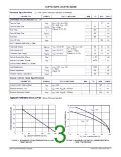
THERMAL SPECIFICATIONS
Thermal Resistance Junction to Case
Thermal Resistance Junction to Ambient
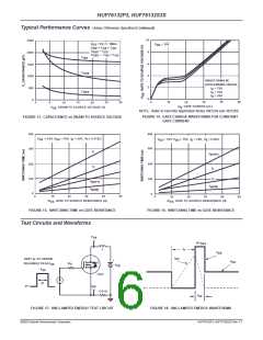
SWITCHING SPECIFICATIONS (VGS = 4.5V)
Turn-On Time
o
R
R
(Figure 3)
TO-220, TO-262 and TO-263
-
-
-
-
1.03
62
C/W
θJC
o
C/W
θJA
t
V
R
= 15V, I
41A,
= 0.366Ω, V = 4.5V,
GS
-
-
-
-
-
-
-
17
105
33
42
-
185
ns
ns
ns
ns
ns
ns
ON
DD
D
L
Turn-On Delay Time
t
-
d(ON)
R
= 6.2Ω
GS
(Figures 15, 21, 22)
Rise Time
t
-
r
Turn-Off Delay Time
t
-
-
d(OFF)
Fall Time
t
f
Turn-Off Time
t
113
OFF
©2003 Fairchild Semiconductor Corporation
HUF76132P3, HUF76132S3S Rev. C1

 FAIRCHILD [ FAIRCHILD SEMICONDUCTOR ]