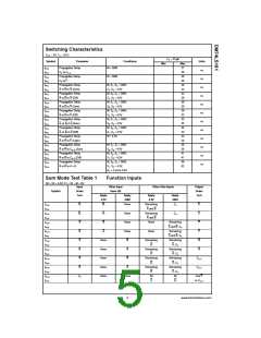
Diff Mode Test Table 2
S1 = S2 = 4.5V, S0 = S3 = M = 0V
Function Inputs
Input
Other Input
Same Bit
Other Data Inputs
Output
Under
Test
Symbol
Under
Test
Apply
Apply
GND
Apply
Apply
GND
4.5V
4.5V
t
t
A
B
A
B
A
B
A
B
A
B
None
B
Remaining
A
Remaining
F
i
PLH
PHL
B, C
n
t
t
A
None
A
None
B
Remaining
A
Remaining
B, C
F
i
PLH
PHL
n
t
t
None
None
None
None
Remaining
A and B, C
P
P
PLH
PHL
n
t
t
None
None
A
Remaining
A and B, C
PLH
PHL
n
t
t
B
Remaining
A and B, C
G
PLH
PHL
n
t
t
None
None
A
Remaining
A and B, C
G
PLH
PHL
n
t
t
B
Remaining
A
Remaining
B, C
A = B
A = B
PLH
PHL
n
t
t
None
None
Remaining
A
Remaining
B, C
PLH
PHL
n
t
t
B
None
Remaining
A and B, C
C
PLH
PHL
n+4
n
t
t
t
t
None
None
A
None
Remaining
C
C
PLH
PHL
PLH
PHL
n+4
n+4
A and B, C
None
n
C
None
All
n
A and B
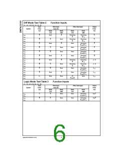
Logic Mode Test Table 3
S1 = S2 = M = 4.5V, S0 = S3 = 0V
Function Inputs
Input
Other Input
Same Bit
Apply
Other Data Inputs
Output
Under
Test
Symbol
Under
Test
Apply
4.5V
B
Apply
4.5V
Apply
GND
GND
t
t
t
t
A
B
None
None
Remaining
A and B, C
Any F
Any F
PLH
PHL
n
A
None
None
Remaining
A and B, C
PLH
PHL
n
www.fairchildsemi.com
6

 FAIRCHILD [ FAIRCHILD SEMICONDUCTOR ]