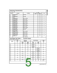
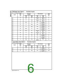
Switching Characteristics
V
CC = 5V, T = 25°C
A
C
= 15 pF
L
Symbol
Parameter
Conditions
Units
ns
Min
Max
27
20
26
20
29
23
32
26
30
30
30
33
32
25
32
33
33
29
38
38
41
41
50
62
t
Propagation Delay
C to C
n
M = GND
M = GND
PLH
t
PHL
n+4
t
Propagation Delay
C to F
n
PLH
ns
t
PHL
t
Propagation Delay
A or B to G (Sum)
Propagation Delay
A or B to G (Diff)
Propagation Delay
A or B to P (Sum)
Propagation Delay
A or B to P (Diff)
Propagation Delay
M, S , S = GND;
1 2
PLH
ns
t
S , S = 4.5V
1 3
PHL
t
M, S , S = GND;
0 3
PLH
ns
t
S , S = 4.5V
1 2
PHL
t
M, S , S = GND;
1 2
PLH
ns
t
S , S = 4.5V
0 3
PHL
t
M, S , S = GND;
0 3
PLH
ns
t
S , S = 4.5V
1 2
PHL
t
M, S , S = GND;
1 2
PLH
ns
t
A or B to F (Sum)
S , S = 4.5V
0 3
PHL
i
i
i
t
Propagation Delay
A or B to F (Diff)
M, S , S = GND;
0 3
PLH
ns
t
S , S = 4.5V
1 2
PHL
i
i
i
t
Propagation Delay
A or B to F (Logic)
Propagation Delay
M = 4.5V
PLH
ns
t
PHL
t
M, S , S = GND;
1 2
PLH
ns
t
A or B to C
(Sum)
S , S = 4.5V
0 3
PHL
n+4
t
Propagation Delay
A or B to C (Diff)
M, S , S = GND;
0 3
PLH
ns
t
S , S = 4.5V
1 2
PHL
n+4
t
Propagation Delay
M, S , S = GND;
0 3
PLH
ns
t
A or B to A = B
S , S = 4.5V;
PHL
1
2
R
= 2 kΩ to 5.0V
L
Sum Mode Test Table 1
S0 = S3 = 4.5V, S1 = S2 = M = 0V
Function Inputs
Input
Other Input
Same Bit
Other Data Inputs
Output
Symbol
Under
Test
Under
Test
Apply
4.5V
Apply
GND
Apply
Apply
GND
4.5V
Remaining
A and B
Remaining
A and B
None
t
A
B
B
None
C
F
i
PLH
PHL
i
i
n
t
t
t
t
t
t
t
t
t
t
t
t
t
t
t
t
t
A
None
None
None
B
C
F
i
PLH
PHL
i
i
n
A
B
A
B
A
B
B
Remaining
A and B, C
P
P
PLH
PHL
n
A
None
Remaining
A and B, C
PLH
PHL
n
None
None
None
None
None
Remaining
Remaining
A, C
G
G
PLH
PHL
B
n
A
Remaining
Remaining
A, C
PLH
PHL
B
n
B
Remaining
Remaining
A, C
C
PLH
PHL
n+4
n+4
B
n
A
Remaining
Remaining
C
PLH
PHL
B
All
A
A, C
All
n
C
None
Any F
or C
PLH
PHL
n
B
n+4
5
www.fairchildsemi.com

 FAIRCHILD [ FAIRCHILD SEMICONDUCTOR ]